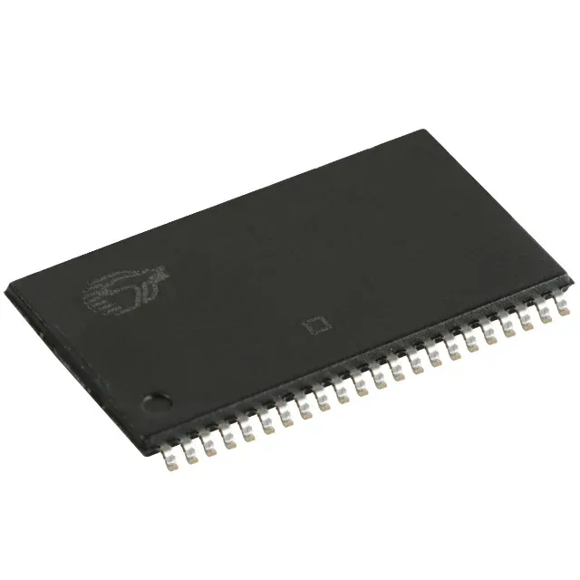
Infineon Technologies CY7C1020CV33-15ZSXE — Memory (DRAM / SRAM / Flash / EEPROM)

CY7C1020CV33-15ZSXE Infineon 512Kbit SRAM, 15ns, 44-TSOP

MPNCY7C1020CV33-15ZSXE
Obsolete

Infineon Technologies CY7C1020CV33-15ZSXE, asynchronous SRAM, 512Kbit (32K x 16), 15 ns access time, 3V-3.6V supply, -40°C to 125°C, 44-TSOP II, Tube.

Sourced new & surplus through independent channelsAuthenticity-screened · ESD-safe packingListing updated Jul 2026

Specifications

CY7C1020CV33-15ZSXE specifications
ParameterValue
Memory typeVolatile
MountingSurface Mount
Voltage3V ~ 3.6V
Memory interfaceParallel
Operating temperature-40°C~125°C(TA)
PackageTube
TechnologySRAM - Asynchronous
Access time15 ns
Memory size512Kbit
Memory formatSRAM
Case44-TSOP (0.400\", 10.16mm Width)
Memory organization32K x 16
Write cycle time - word, page15ns

Product details

512Kbit asynchronous SRAM — obsolete, sourced to order

The CY7C1020CV33-15ZSXE: The 15 ns access and write cycle times suit it for processor local-bus or cache-tag applications where the read latency must stay under one bus clock at moderate frequencies.

Temperature grade and supply — industrial floor to ceiling

Parallel interface with a 15 ns write cycle — the data sheet specifies word and page write timing, so the controller must hold address and data valid for the full 15 ns window.

Package — 44-TSOP II, surface-mount layout

Housed in a 44-TSOP II (0.400-inch body width, 10.16 mm), the package is a standard JEDEC outline for mid-density asynchronous SRAMs — the 0.8 mm pin pitch is hand-solderable but best reflowed with a profile peaking at 245°C peak for lead-free assemblies. Supplied in Tube format — not tape-and-reel, so pick-and-place lines need a tube feeder or manual loading for prototype runs.

Frequently asked questions

What is the access time and memory organization of this SRAM?

15 ns access time, organized as 32K x 16 bits (512Kbit total). The write cycle time is also 15 ns for word and page writes.

What package does CY7C1020CV33-15ZSXE use?

44-TSOP II (0.400-inch body, 10.16 mm width) — a standard JEDEC surface-mount outline for asynchronous SRAMs. Supplied in Tube format.