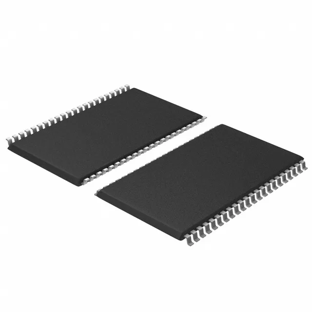
Infineon Technologies CY7C1020CV26-15ZSXE — Memory (DRAM / SRAM / Flash / EEPROM)

CY7C1020CV26-15ZSXE SRAM, 512Kbit, 15 ns, 44-TSOP II

MPNCY7C1020CV26-15ZSXE
Last Buy

Infineon CY7C1020CV26-15ZSXE, asynchronous SRAM, 512Kbit (32K x 16), 15 ns access time, parallel interface, 2.5V–2.7V supply, -40°C to 125°C, 44-TSOP II (0.400", 10.16mm width), surface mount, tray.

$4.2896Ref. price · indicative, final on quote
Independent supplier — new & surplus stockAuthenticity-screened · ESD-safe packingListing updated Jul 2026

Specifications

CY7C1020CV26-15ZSXE specifications
ParameterValue
Memory typeVolatile
MountingSurface Mount
Voltage2.5V ~ 2.7V
Memory interfaceParallel
Operating temperature-40°C ~ 125°C (TA)
PackageTray
TechnologySRAM - Asynchronous
Access time15 ns
Memory size512Kbit
Memory formatSRAM
Case44-TSOP (0.400\", 10.16mm Width)
Memory organization32K x 16
Write cycle time - word, page15ns

Product details

512Kbit asynchronous SRAM for industrial and automotive cache buffers

It operates from a 2.5V to 2.7V supply rail — narrow enough that a dedicated LDO is the cleanest way to feed it, especially if the board's main 3.3V or 1.8V rail doesn't overlap.

The parallel interface is straightforward to hook up — address, data, chip enable, output enable, and write enable — no clock or refresh overhead. The 2.5V to 2.7V supply means the I/O levels are not 3.3V tolerant; a level shifter or a 2.5V-logic host is needed.

Last Buy — secure stock before the window closes

Once that window shuts, new-manufactured units will no longer be available.

44-TSOP II footprint and storage notes

The 44-TSOP II package (0.400" body width, 10.16 mm) is a standard JEDEC outline shared by many 512Kbit and 1Mbit asynchronous SRAMs, so the board footprint is reusable if you need to qualify a second source.

Frequently asked questions

What is the access time of CY7C1020CV26-15ZSXE?

This allows zero-wait-state operation with a 33 MHz bus and one wait state at 66 MHz.