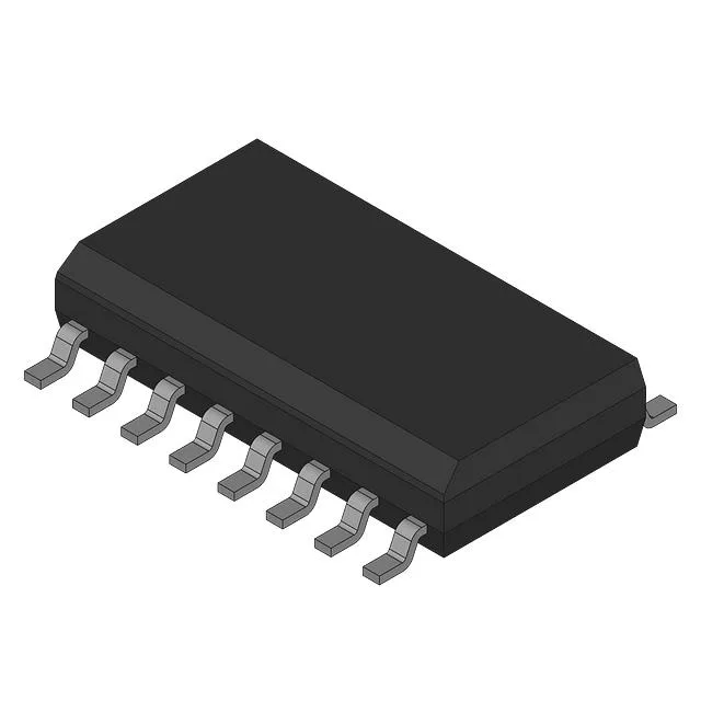
Infineon Technologies CY7C1019DV33-10ZSXI — Memory (DRAM / SRAM / Flash / EEPROM)

CY7C1019DV33-10ZSXI SRAM 1Mbit 10 ns Asynchronous, Obsolete

MPNCY7C1019DV33-10ZSXI
Obsolete

Cypress CY7C1019DV33-10ZSXI, 1Mbit asynchronous SRAM, 128K x 8 organization, 10 ns access time, 3V to 3.6V supply, -40°C to 85°C, 32-TSOP II package, Tray.

$6.1334Ref. price · indicative, final on quote
Independent supplier — new & surplus stockAuthenticity-screened · ESD-safe packingListing updated Jul 2026

Specifications

CY7C1019DV33-10ZSXI specifications
ParameterValue
Memory typeVolatile
MountingSurface Mount
Voltage3V ~ 3.6V
Memory interfaceParallel
Operating temperature-40°C ~ 85°C (TA)
PackageTray
TechnologySRAM - Asynchronous
Access time10 ns
Memory size1Mbit
Memory formatSRAM
Case32-SOIC (0.400\", 10.16mm Width)
Memory organization128K x 8
Write cycle time - word, page10ns

Product details

What this 1Mbit asynchronous SRAM does in a design

As an asynchronous part, it requires no clock — the read and write cycles are triggered by address transitions and control strobes, which simplifies the memory controller design but limits burst throughput compared to synchronous SRAMs. This part is suited for applications that need fast, random-access scratchpad memory without the complexity of a clocked interface: networking equipment, industrial controllers, test instrumentation, and embedded systems where the bus master can tolerate single-cycle handshakes.

10 ns access time — timing budget for the bus

On a 100 MHz bus (10 ns period), this SRAM leaves essentially zero margin for address-to-data setup before the next clock edge — the bus controller must insert at least one wait state or use a slower clock domain. For a 50 MHz bus (20 ns period), the 10 ns access gives a comfortable 10 ns of setup margin before the next rising edge, allowing zero-wait-state reads if the controller's address-to-output delay is accounted for. When sizing the memory subsystem, factor in the controller's own propagation delays and the PCB trace flight time; a 10 ns part on a 66 MHz bus (15 ns period) typically needs one wait state.

For new designs, a pin-compatible alternative should be qualified.

Package and footprint — 32-TSOP II wide body

The package ships in Tray form. For rework, the wide SOIC-like body is compatible with standard hot-air profiles;.

Frequently asked questions

Is CY7C1019DV33-10ZSXI obsolete?

Yes, Cypress has marked this part as obsolete. There is no official replacement listed in the available records.

How fast is the CY7C1019DV33-10ZSXI?

The access time is 10 ns, and the write cycle time (word or page) is also 10 ns. This means the part can complete a read or write operation in 10 ns from the address or control strobe, which is typical for a fast asynchronous SRAM in this density range.

What is the replacement for CY7C1019DV33-10ZSXI?

The CY7C1018DV33-10VXI is a 1Mbit asynchronous SRAM with the same 10 ns access time and 128K x 8 organization, but it ships in a different package (Tube vs Tray) and may have minor parametric differences — verify pin compatibility and timing before substituting.