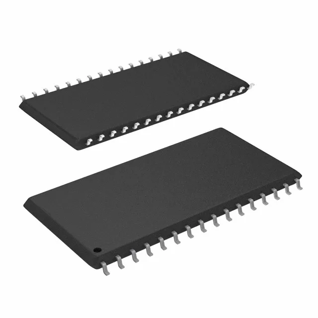
1 Mbit async SRAM for legacy bus interfaces
The CY7C1019CV33-10ZXI is a 1 Mbit asynchronous SRAM organized as 128K x 8 bits, with a 10 ns access time that matches the bus timing of legacy 8-bit microcontrollers and DSPs without wait states.
No official successor or pin-compatible replacement is recorded from Infineon for this specific variant. No stock-holding claim — sourced per request.
The 32-TSOP II (thin small-outline package) footprint is 0.400" wide, 10.16 mm, with a standard 0.50 mm pin pitch — a common layout for 8-bit wide SRAM on two-layer boards. Supplied in tray packaging, suitable for hand assembly or low-volume reflow; not tape-and-reel for automated pick-and-place.
Timing and bus interface
Both the access time and the write cycle time (word, page) are specified at 10 ns, so the part can sustain back-to-back read or write operations at 100 MHz bus clock without dead cycles. The parallel memory interface is asynchronous — no clock input required — simplifying the PCB layout by eliminating a routed clock trace to the SRAM.