1Mbit asynchronous SRAM with 12 ns access — what the timing means for the bus
The Infineon CY7C1019B-12ZXC is a 1Mbit asynchronous SRAM organized as 128K x 8 bits, with a 12 ns access time and a 12 ns write cycle time. The 12 ns access time means the part can complete a read operation within 12 ns of the address being valid — fast enough to interface with many 5V CPLDs, legacy ASICs, and 8-bit microcontrollers without inserting wait states, as long as the bus timing budget accounts for address-to-data setup. The parallel interface is straightforward: no clock, no burst mode — the chip select and output enable gates the data bus directly. If your system runs a mixed 3.3 V/5 V bus, the SRAM's inputs are 5 V-tolerant only within its own supply range — level translation on the address and control lines is required when the controller is 3.3 V.
Obsolete — planning the BOM line
The CY7C1019B-12ZXC carries an official product status of Obsolete. No last-time-buy window or successor part number is recorded in the available lifecycle data. A design that needs ongoing production should plan for a pin-compatible replacement or a board respin to a current-generation asynchronous SRAM.
Package and footprint — 32-SOIC wide body
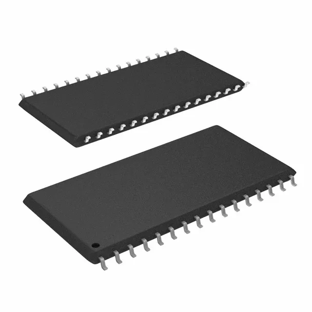
The package is a 32-SOIC with a 0.400-inch (10.16 mm) body width, surface mount. This is not the same footprint as the narrow 0.300-inch SOIC-32 or the thin TSOP-I variants — a board layout using this part cannot drop in a narrow SOIC without a PCB change. The shipping medium is tray, not tape and reel, which may affect pick-and-place feeder setup for high-volume lines.