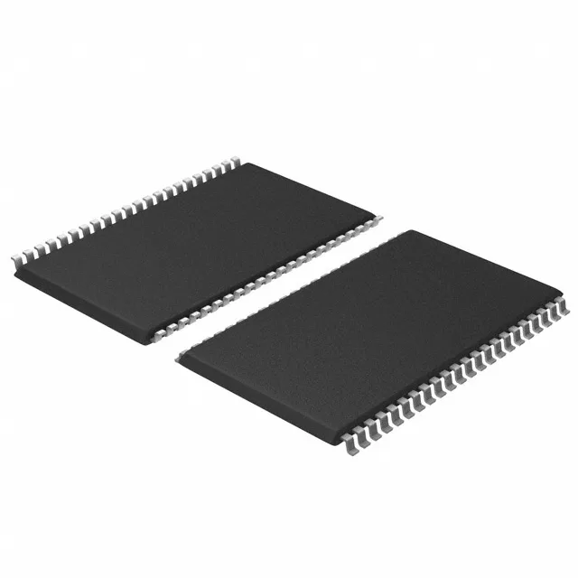
Infineon Technologies CY7C1011G30-12ZSXET — Memory (DRAM / SRAM / Flash / EEPROM)

CY7C1011G30-12ZSXET Infineon 2Mbit Async SRAM, 10 ns

MPNCY7C1011G30-12ZSXET
Active

Infineon CY7C1011G30-12ZSXET, asynchronous SRAM, 2Mbit (128K x 16), 10 ns access time, parallel interface, 2.2V to 3.6V supply, -40°C to 125°C, 44-TSOP II, Tape & Reel.

$8.6625Ref. price · indicative, final on quote
Independent supplier — new & surplus stockAuthenticity-screened · ESD-safe packingListing updated Aug 2026

Specifications

CY7C1011G30-12ZSXET specifications
ParameterValue
Memory typeVolatile
MountingSurface Mount
Voltage2.2V ~ 3.6V
Memory interfaceParallel
Operating temperature-40°C~125°C(TA)
PackageTape & Reel (TR)
TechnologySRAM - Asynchronous
Access time10 ns
Memory size2Mbit
Memory formatSRAM
Case44-TSOP (0.400\", 10.16mm Width)
Memory organization128K x 16
Write cycle time - word, page10ns

Product details

2Mbit asynchronous SRAM in 44-TSOP II — fit check for the memory bus

The 10 ns access and write-cycle times give the bus a tight timing budget — the memory controller must have a setup-and-hold window that closes within that window, so verify the controller's AC timing against the datasheet's derating curves at your operating voltage and temperature.

For a production BOM, this means no forced requalification or redesign cycle in the near term — but as with any active semiconductor, monitor PCNs for package or wafer-fab changes that could affect timing or supply continuity.

Package and mounting — 44-TSOP II on the board

The TSOP II footprint is a standard SRAM layout shared across many 2Mbit and 4Mbit asynchronous parts from multiple vendors, so a board designed for a compatible TSOP II SRAM should accept this device without a layout change.

Frequently asked questions

What is the memory technology and organization of CY7C1011G30-12ZSXET?

It is an asynchronous SRAM with a 2Mbit density organized as 128K x 16 bits, using a parallel interface. The access time and write-cycle time are both 10 ns.