10 ns asynchronous SRAM for high-speed buffering
The parallel interface and 2.2V to 3.6V supply range let it drop into 3.3V or 2.5V memory buses without extra level shifting.
10 ns access time — timing margin in the bus
In a system with a 100 MHz bus, that leaves about 10 ns of setup margin before the next clock edge — enough for a single load but tight if the bus fans out to multiple memories. For a design already running a 66 MHz or slower bus, the 10 ns window gives comfortable headroom for PCB trace delays and capacitive loading.
2Mbit density and 128K x 16 organization
The 128K x 16 organization means the part presents a 16-bit-wide data bus, which matches the native word width of many 16-bit MCUs and DSPs. For a 32-bit processor, two of these parts can pair to form a 32-bit wide memory bank. The 2Mbit capacity is enough for moderate-sized frame buffers, parameter tables, or boot-code shadowing in systems where an external SRAM offloads the main processor's internal RAM.
48-FBGA package and layout considerations
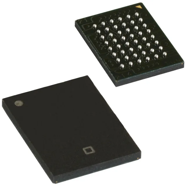
The 48-FBGA uses a 6x8 ball matrix; the datasheet's recommended land pattern and via fanout should be followed exactly to avoid solder-bridge or open joints.