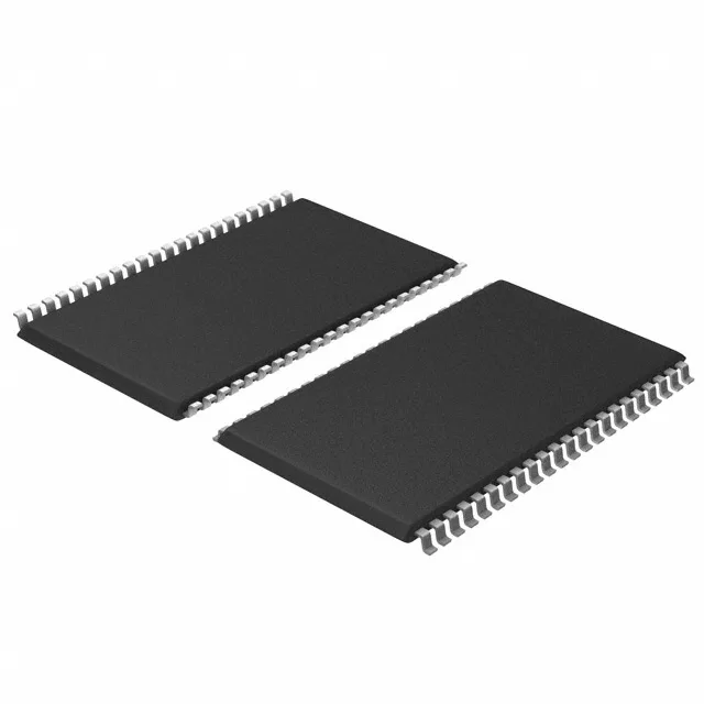
128K x 16 asynchronous SRAM — 10 ns access, 3.3 V core
The CY7C1011CV33-10ZSXAT is a 2 Mbit asynchronous SRAM organized as 128K words by 16 bits. The parallel interface and 10 ns access time place it in the fast-page SRAM class, suitable for cache, buffer, or scratchpad memory in embedded systems where deterministic read/write latency matters more than serial-bus throughput.
10 ns access — timing margin in the memory bus
Both the address-to-data access time and the write cycle time are specified at 10 ns. For a 100 MHz bus clock with a 10 ns period, this SRAM leaves zero margin for address-to-data setup in a single-cycle read — the controller must insert a wait state or use a pipelined access scheme. At 66 MHz (15 ns period), the 10 ns access provides 5 ns of timing slack before the data latch edge. The write cycle time of 10 ns means the minimum write pulse width is also 10 ns. The controller's write strobe must meet this minimum; a shorter pulse risks incomplete data capture, especially at the temperature extremes where the SRAM's internal timing shifts.
44-TSOP II — board integration and rework
The 10.16 mm width fits standard SOIC-44 footprints, but the TSOP II body is thinner — verify the solder-paste stencil aperture against the land pattern to avoid bridging on the fine-pitch leads. Supplied in Tape & Reel (TR), the part is ready for pick-and-place assembly in volume production. The reel quantity is not specified here, but TSOP II reels typically carry 1,000 or 2,000 units per reel depending on tape width.
Active lifecycle — sourcing posture
Infineon lists the CY7C1011CV33-10ZSXAT as Active.