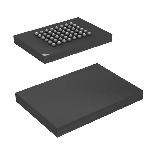
Infineon Technologies CY7C1011CV33-10BAJXE — Memory (DRAM / SRAM / Flash / EEPROM)

Infineon CY7C1011CV33-10BAJXE 2Mbit Async SRAM, 10 ns

MPNCY7C1011CV33-10BAJXE
End of Life

Infineon CY7C1011CV33-10BAJXE, asynchronous SRAM, 2Mbit (128K x 16), parallel interface, 10 ns access time, 3V to 3.6V supply, -40°C to 125°C, 48-TFBGA, Tray.

$2.2200Ref. price · indicative, final on quote
Independent supplier — new & surplus stockAuthenticity-screened · ESD-safe packingListing updated Aug 2026

Specifications

CY7C1011CV33-10BAJXE specifications
ParameterValue
Memory typeVolatile
MountingSurface Mount
Voltage3V ~ 3.6V
Memory interfaceParallel
Operating temperature-40°C ~ 125°C (TA)
PackageTray
TechnologySRAM - Asynchronous
Access time10 ns
Memory size2Mbit
Memory formatSRAM
Case48-TFBGA
Memory organization128K x 16
Write cycle time - word, page10ns

Product details

The CY7C1011CV33-10BAJXE is a 2Mbit asynchronous SRAM from Infineon (formerly Cypress), organized as 128K words by 16 bits. It uses a parallel interface and delivers a 10 ns access time, which sets the timing budget for address-to-data valid on the bus. At 3.3 V nominal (3V to 3.6V range), this part is a drop-in for designs needing fast, simple memory without a clock — no refresh, no setup sequences.

The 10 ns access time is specified across that full range, so timing closure at 125°C uses the same margin as at 25°C. No derating needed for temperature; the part is characterized for it.

Package and supply — layout notes

The 48-TFBGA (6x8 mm) is a fine-pitch ball grid array; the balls are under the package, so routing escapes on a two-layer board are tight — expect to use micro-vias or at least four layers for clean signal routing. Decouple with a 0.1 µF ceramic per supply pin, placed as close to the balls as the layout allows. The write cycle time matches the access time at 10 ns, so back-to-back writes run at the same speed as reads.

Frequently asked questions

What is the exact memory organization and interface of CY7C1011CV33-10BAJXE?

It is organized as 128K words by 16 bits (128K x 16) and uses a parallel memory interface. The access time is 10 ns for both read and write cycles.

What are compatible or alternative parts to CY7C1011CV33-10BAJXE?

Pin-compatible alternatives within the same Cypress/Infineon family include other 2Mbit asynchronous SRAMs in the 48-TFBGA package with matching 128K x 16 organization, such as the CY7C1011CV33-10BAJX (without the 'E' suffix, which may denote a different lead-free or tray variant). Verify the exact suffix and datasheet for timing and supply compatibility before substituting.