What the 10 ns access time means for bus timing
The CY7C1007D-10VXI is a 1 Mbit asynchronous SRAM organized as 1M x 1 bit — a single-bit-wide data bus, so each read or write cycle transfers one bit per access. The 10 ns access time sets the window from address valid to data valid on the bus; a 100 MHz controller with a 10 ns clock period has zero margin for address-to-data propagation through the SRAM, so this part pairs best with slower bus controllers or wait-state insertion. The parallel interface and 10 ns write cycle time (word/page) mean the bus timing for writes matches the read speed — no asymmetry to manage in the controller's state machine.
At 85°C ambient, the junction temperature stays within the 125°C abs-max limit for the 28-SOJ package as long as the board copper pour under the SOJ body provides a thermal path. No heatsink needed at this density — the 1 Mbit array draws well under 1 W in active operation.
Infineon lists the CY7C1007D-10VXI as obsolete. The part is sourced through independent distribution — quantities are lot-specific and confirmed at RFQ. For a BOM line that requires this exact 1M x 1 asynchronous SRAM in 28-SOJ, the procurement path is surplus or broker inventory. The 10 ns access time and 5 V supply rail narrow the field — any substitute must match the 28-SOJ footprint, the 4.5 V–5.5 V range, and the parallel interface.
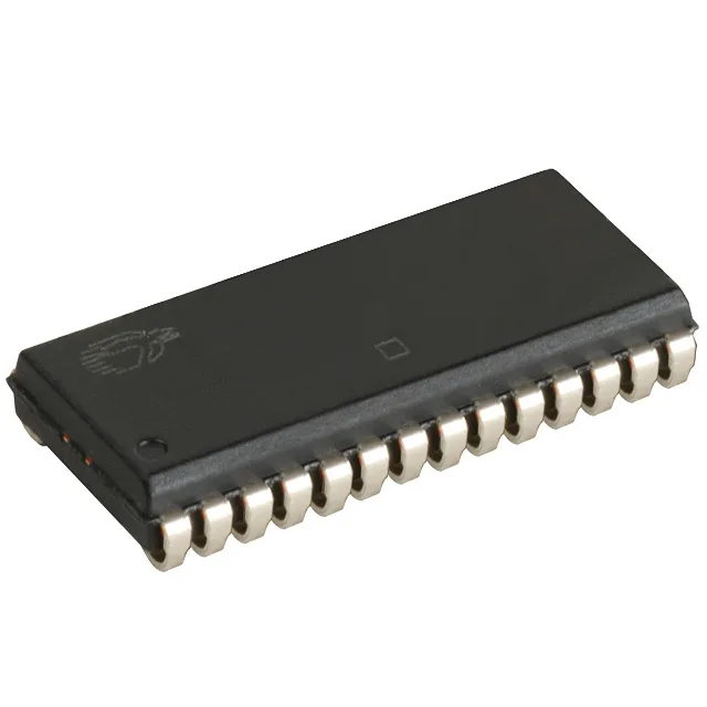
The J-lead profile gives a small solder fillet compared to a gull-wing — the land pattern should extend 0.5 mm beyond the lead toe for a reliable fillet. No exposed pad; all thermal dissipation is through the leads and the board copper. Tube packaging — the parts ship in anti-static tubes, not tape-and-reel. For pick-and-place, the tube must be fed through a tube feeder or the parts transferred to a tray. The 28-SOJ body is compatible with standard JEDEC tube dimensions.