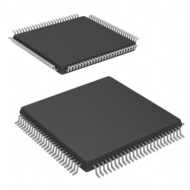
Obsolete — lifecycle reality for the BOM line
The CY7C09379V-6AXC carries an Obsolete product status from Infineon Technologies. This means the manufacturer has ended production; no new orders are accepted at the factory.
This is a 576Kbit synchronous dual-port SRAM organized as 32K words by 18 bits. The dual-port architecture allows two independent controllers or processors to access the same memory array simultaneously through separate address, data, and control buses — a common topology in shared-memory systems like baseband processors, video frame buffers, and multi-core communication bridges. The 6.5 ns access time and 100 MHz clock rate set the timing budget: at 100 MHz the port cycle is 10 ns, so the 6.5 ns access leaves 3.5 ns of margin for address hold, data setup, and board trace delay before the next clock edge. This margin shrinks with capacitive loading on the parallel bus — the 100-TQFP package's 0.5 mm pitch trace routing and the number of loads on the data bus determine whether the timing closes in a given layout. Supply voltage range is 3V to 3.6V, which aligns with a 3.3V nominal rail. The commercial temperature grade (0°C to 70°C) limits the part to indoor, controlled-environment equipment — not suitable for extended outdoor, industrial, or automotive deployment without thermal qualification.
100-TQFP package — board integration note
Housed in a 100-lead LQFP (supplier device package 100-TQFP, 14x14 mm body). The exposed paddle is not present on this QFP; thermal dissipation relies on the leadframe and board copper.