12 ns access, 50 MHz arbitration clock
The CY7C09379V-12AC is a dual-port synchronous SRAM organized 32K x 18 bits, with a 12 ns access time and a 50 MHz clock. The 18-bit word width maps naturally to a 16-bit data bus with two parity bits, or to an 18-bit DSP data path where the extra two bits carry a tag or ECC syndrome.
Dual-port architecture — what it means for the bus
Both ports are independent and synchronous, each with its own address, data, and control lines. The 12 ns access time sets the window for the arbitration handshake — when both ports address the same memory location in the same clock cycle, the internal arbiter grants one side and flags the collision on the other. The 50 MHz clock limits the arbitration cycle to 20 ns, so the 12 ns access leaves 8 ns of setup/hold margin at the bus interface. The 32K x 18 organization means 32,768 addressable locations, each 18 bits wide. Total memory is 576 Kbit. For a 16-bit processor with parity, the full 18-bit word is consumed by data plus two parity bits; for an 18-bit DSP, every bit is payload.
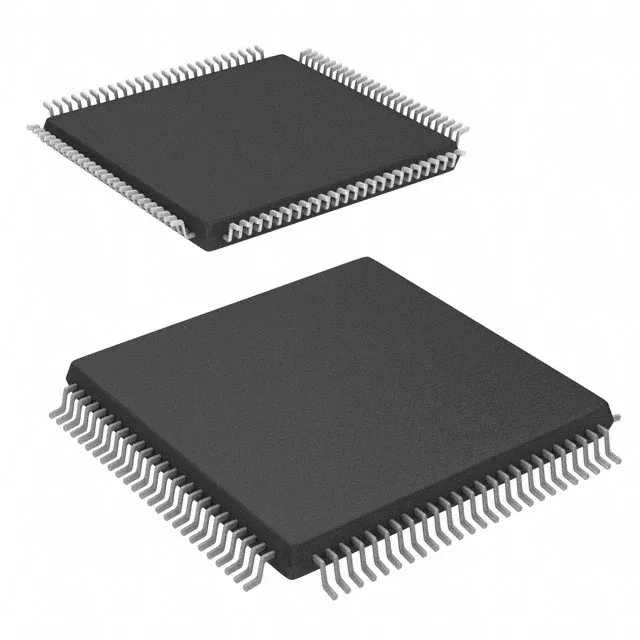
The 100-TQFP (14x14 mm, 0.5 mm pitch) package is a standard JEDEC footprint. If a board spin is an option, a pin-compatible dual-port SRAM from the same Cypress/Infineon family (base number CY7C09379) may still be active — verify the specific speed grade and temperature range against the BOM requirement.
The tray packaging is standard for this form factor. Surface-mount assembly follows standard JEDEC MSL-3 moisture sensitivity — a bake step is required if the tray seal is broken and the floor life is exceeded.