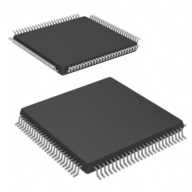
What the 12 ns access time and 50 MHz clock mean for arbitration
The CY7C09199V-12AXC is a synchronous dual-port SRAM organized 128K x 9 — the ninth bit is typically the parity lane for data-integrity checking in telecom or industrial backplane buffers. 12 ns access time means the read data appears on the bus within 12 ns of the clock edge that initiates the cycle — this sets the arbitration window when both ports contend for the same memory location. 50 MHz clock frequency gives a 20 ns cycle time; the 12 ns access leaves 8 ns of bus turnaround margin before the next clock edge, which is tight for back-to-back reads on a shared bus without wait states.
Obsolete — sourcing through surplus and broker channels
No pin-compatible replacement from Infineon is documented; a board spin or a parametric search for a 128K x 9 synchronous dual-port SRAM in a 100-pin QFP package is the migration path for new designs.
Package and supply rail — board-fit checklist
100-LQFP package (also specified as 100-TQFP 14x14 mm) — the 0.5 mm pitch demands a controlled-impedance PCB stack-up if the bus runs above 40 MHz; the 50 MHz clock rate puts the third harmonic at 150 MHz, where trace stubs longer than 5 mm cause reflections. Commercial temperature grade (0°C to 70°C) limits deployment to controlled indoor environments — no extended industrial or automotive qualification on this variant.