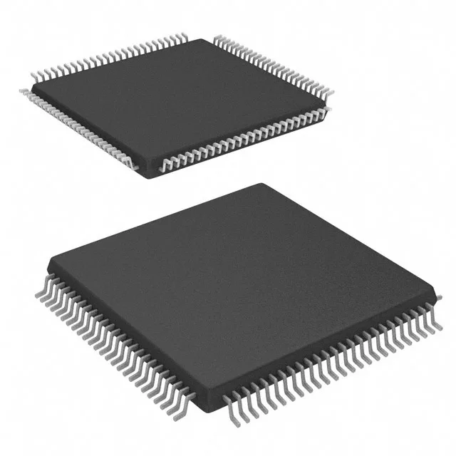
The Cypress CY7C09159AV-9AXC is a 72Kbit synchronous dual-port SRAM organized as 8K x 9 bits. It provides two independent ports with separate address, data, and control lines, allowing simultaneous read/write access from two bus masters. The 9 ns access time and 67 MHz clock rate suit shared-memory applications like multiprocessor buffers, FIFO emulation, or mailbox registers in telecom and datacom equipment. The 100-pin TQFP package (14x14 mm) is a surface-mount footprint common in mid-density board designs.
9 ns access and 67 MHz — what they mean for bus timing
In a synchronous dual-port, this sets the minimum read-cycle window for the slower port. The 67 MHz clock defines the maximum arbitration rate: each port can perform a read or write every 14.9 ns. A designer sizing the bus margin should budget for the sum of access time, trace delay, and setup time of the receiving device. The 9 ns rating leaves about 6 ns for board parasitics and logic at 67 MHz, which is workable on a well-laid-out four-layer PCB.
8K x 9 organization — why the extra bit
The 9-bit width (8 data bits plus one parity or control bit) is a legacy telecom and networking convention. The ninth bit often carries a parity flag or a start-of-packet marker in HDLC-style controllers. If the design uses only 8-bit data, the ninth bit can be tied low or left unconnected, but the memory depth is fixed at 8K words. For a pure 8-bit application, a standard 8-bit-wide dual-port (e.g., 8K x 8) would waste no bits, but the 9-bit organization is a deliberate fit for designs already using the ninth line.
Sourcing is through independent distribution and surplus channels. Buyers should verify date-code provenance and inspect for counterfeits — this part's age makes it a target for re-marked or salvaged stock.