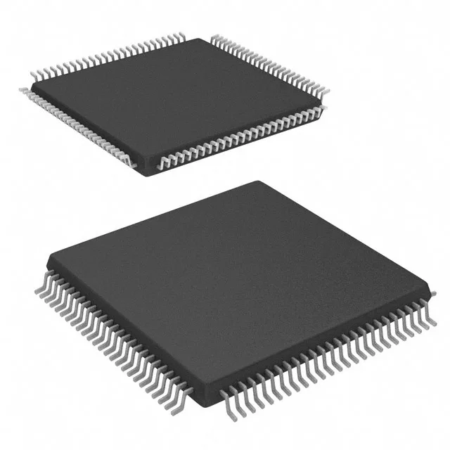
1 Mbit synchronous dual-port SRAM — 6.5 ns access, 100 MHz clock
The Infineon CY7C09099V-6AXC is a 1 Mbit synchronous dual-port SRAM organized as 128K x 8. It provides two independent ports with separate address, data, and control lines, allowing simultaneous read/write access from two bus masters or processors.
6.5 ns access time — timing margin for the shared bus
The 6.5 ns access time at 100 MHz clock gives the designer a 10 ns cycle window. The dual-port architecture eliminates the arbitration overhead of multiplexed single-port SRAM, but the 6.5 ns output-enable-to-data-valid window still needs to clear the setup time of the receiving FPGA or ASIC. With a 100 MHz bus, the timing budget after trace delay and clock skew runs tight — the 6.5 ns figure is the headline number, but the real margin depends on the output hold time and the load capacitance on the data lines.
Obsolete — no direct Infineon replacement on record
Infineon has not published a direct pin-compatible successor for this specific dual-port synchronous SRAM. The 100-TQFP footprint and 3.3 V supply rail are common enough that a cross-ship against a known-good date code lot is the practical path — there is no drop-in replacement from the same manufacturer.
100-TQFP (14x14) — footprint and storage
The 100-TQFP (14x14) package is a standard fine-pitch quad flat pack. The Tray shipping medium means the parts arrive in antistatic trays, not tape-and-reel. For the storeroom, these trays stack neatly but take up more shelf space per unit than a reel. Store the trays dry with desiccant and a humidity indicator card.
It will not survive an unheated enclosure, engine bay, or outdoor cabinet without a heater.