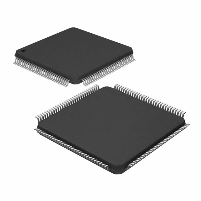
The Cypress CY7C0831AV-133AXI is a 2Mbit synchronous dual-port SRAM organized as 128K x 18 bits, clocked at 133 MHz. The synchronous interface latches addresses on the clock edge, so timing closure at 133 MHz demands careful PCB layout and matched trace lengths on the address and control lines.
133 MHz clock — timing margin and bus design
At 133 MHz the clock period is about 7.5 ns. The datasheet's AC timing parameters — tCO (clock to output), tDS (data setup), tDH (data hold) — define the window you have to capture read data and meet write setup. With a typical FPGA or ASIC interface, you'll want to budget at least 1 ns of PCB flight time and derate for the industrial temperature range.
The 120-TQFP package (14x14 mm) is a fine-pitch surface-mount footprint — MSL 3 moisture sensitivity, so bake before reflow if the moisture-barrier bag has been open longer than the floor-life window.
If your design can tolerate a form-fit-function alternate, the CY7C0831 family includes other density and speed grades that may still be active; check the base product number CY7C0831 for sibling variants.