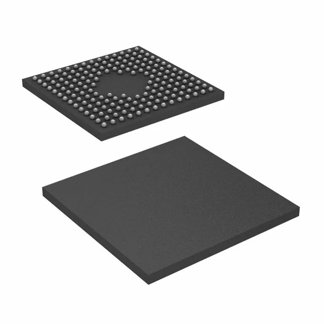
The Infineon CY7C057V-15BBC is a 1.152 Mbit asynchronous dual-port SRAM organized as 32K x 36 bits. It gives two independent systems — two processors, an FPGA and a CPU, or a DSP and a microcontroller — simultaneous read/write access to a shared memory buffer without a multiplexed bus or external arbitration logic. The 15 ns access time means each port can complete a read or write cycle in 15 ns, which translates to a 66 MHz equivalent bus rate for back-to-back accesses. This part is built for shared-memory applications in telecom line cards, baseband processing, video frame buffers, and multiprocessor data-exchange where deterministic latency matters more than peak throughput.
For a design running a 66 MHz bus clock (15 ns period), this part leaves zero margin for address-to-data setup if the bus master drives the address on the same clock edge. In practice, most designs insert one wait state or use the 15 ns write cycle time for pipelined writes. If your system clock is 50 MHz (20 ns period), the 15 ns access gives a comfortable 5 ns margin for PCB trace delay and logic propagation.
32K x 36 organization — wider than the usual 32-bit bus
The 36-bit word width (32K x 36) is wider than the standard 32-bit memory bus. The extra four bits are typically used for parity or ECC storage per word, or as sideband control bits in a FIFO or mailbox implementation. If your system uses a 32-bit data bus with byte enables, the 36-bit width gives you four spare bits that can serve as flags, semaphores, or error-detection codes without stealing data bandwidth. The parallel interface is straightforward — address, data, chip select, output enable, and read/write control on each port — no clock, no burst logic.
The CY7C057V-15BBC operates from 3.0 V to 3.6 V, making it a 3.3 V nominal part. It is not 5 V tolerant on the I/O — level translation is needed if interfacing with 5 V logic. For extended-temperature designs, look at the industrial-grade variants in the CY7C057 family (often suffix -I or -B).
Package and PCB considerations
That is a fine-pitch BGA — standard PCB fabrication handles it (0.2 mm trace/space, microvia recommended for fanout under the balls), but rework requires a hot-air station with a BGA nozzle and a stencil for solder paste. The package is moisture-sensitive; MSL level is not listed here, but typical Infineon LBGAs of this era are MSL 3, meaning a bake before reflow if the sealed bag has been open longer than 168 hours at <30°C/60% RH. The tray shipping medium is standard for BGA devices — no tape-and-reel option is listed.
The CY7C057V-15BBC is marked obsolete by Infineon (formerly Cypress). For new designs, Infineon's current dual-port SRAM portfolio (e.g., the CY7Cxxxx series with synchronous interfaces or higher densities) should be evaluated, but pin-compatibility is not guaranteed — the 172-ball LBGA footprint and 3.3 V supply may carry over, but the interface protocol (asynchronous vs. synchronous) will differ. Buyers should plan for last-time-buy or alternate-sourcing qualification if production volumes are ongoing.