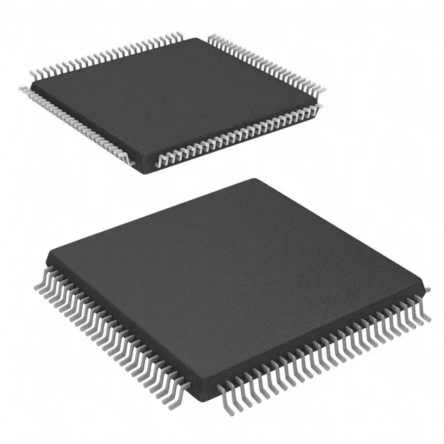
What this dual-port SRAM does that a standard SRAM cannot
The CY7C038V-25AXC from Cypress is a 1.152 Mbit dual-port asynchronous SRAM organized as 64K x 18. Unlike a single-port memory, the dual-port architecture gives two independent buses simultaneous read/write access to the same array — no bus-turnaround dead cycles, no external arbitration logic needed. That makes it the natural fit for a shared mailbox buffer between two processors, a FIFO replacement in a video line buffer, or a rate-matching buffer between a fast DSP and a slower host bus. The 25 ns access time sets the timing budget for both ports. At a 3.3 V nominal supply, that 25 ns window covers address-to-data valid on a read and data setup on a write — tight enough for a 40 MHz bus with reasonable PCB trace delay, but you will want to check hold times against the slower port if the two clock domains are asynchronous. That limits it to indoor, temperature-controlled equipment — office networking gear, test instruments, or telecom line cards in a conditioned central office.
If this SRAM is on your active BOM, you are looking at last-time-buy inventory that has already been produced — once the remaining distributor stock and broker lots are consumed, the part will be unavailable. For a production line that still needs this exact footprint and function, the procurement strategy is to qualify a pin-compatible dual-port SRAM from another vendor, or to secure a multi-year buffer through the surplus channel now. The 100-TQFP dual-port SRAM market has a few cross-shoppable alternatives from Renesas (IDT) and GSI Technology — but each has its own timing and supply voltage variants, so a drop-in swap needs a layout and timing review, not a blind substitution.
3.3 V supply and 25 ns — the timing decisions
It will interface directly with a 3.3 V FPGA, ASIC, or microcontroller without level shifters. The 25 ns access time and 25 ns write cycle time are symmetrical, which simplifies the timing model — both ports run at the same speed. If your system has one port at 40 MHz and the other at 20 MHz, the slower port has plenty of margin; the faster port needs to respect the 25 ns window on every cycle. The 64K x 18 organization gives 18-bit data words — useful for a 16-bit bus plus two parity bits, or for an 18-bit video pixel word. The parallel interface is straightforward: address, data, chip selects, and output enables on each port. No clock, no burst mode — just asynchronous handshaking with the usual SRAM control signals.