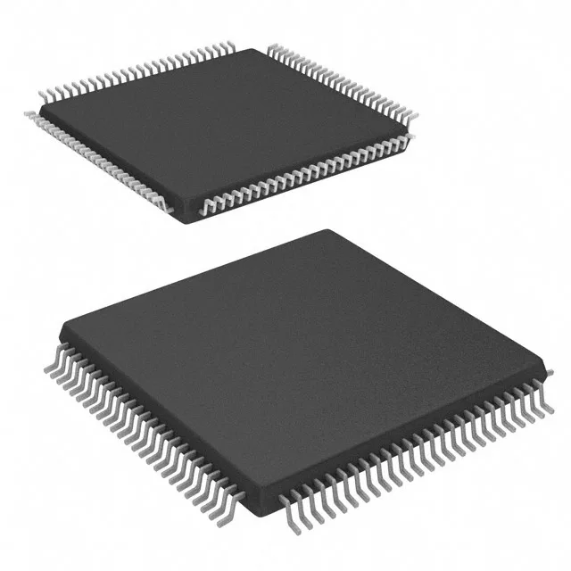
Obsolete dual-port SRAM — what the PCN means for your BOM line
The CY7C037-15AC: This means the manufacturer no longer accepts new orders and no last-time-buy window remains open — any available units are existing inventory from distribution or surplus channels. For a BOM that still calls out this 576Kbit (32K x 18) asynchronous dual-port SRAM, the sourcing path is through independent distribution where date-code-locked lots can be confirmed against the original PCN.
15 ns access time and the bus-margin calculation
In a shared-memory system where two controllers arbitrate for the same SRAM, the 15 ns figure governs the arbitration cycle — a faster master must wait for the full access window or the data bus sees contention. The write cycle time matches the read access at 15 ns, so the memory operates symmetrically — the bus protocol does not need separate timing for read vs write handshake. This simplifies the FPGA or CPLD state machine that manages the dual-port handshake.
100-TQFP footprint and the 5 V supply rail
The 100-TQFP package (14x14 mm body) with 0.5 mm pitch demands a 4-layer PCB for reliable fan-out of the address and data lines — two-layer boards struggle to route 32 address lines plus 18 data lines without via congestion under the package.
It is not rated for industrial enclosures that see freezing starts or summer heat soak above 70°C — a grade 3 or industrial-range SRAM would be needed for those environments.