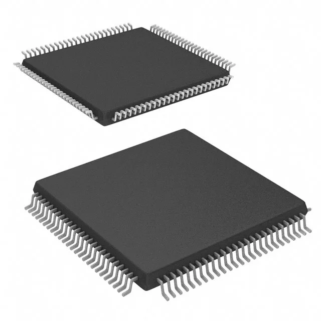
20 ns access, 64K x 16 — the bus-timing fit
The CY7C028V-20AC: The 20 ns access time sets the window between address assertion and valid data on the bus — a 50 MHz controller with 5 ns hold margin needs to budget the full 20 ns plus board trace delay before latching the read word. Organised as 64K words of 16 bits each (1 Mbit total), the memory provides a 16-bit parallel interface that matches a 16-bit data bus without byte-lane multiplexing.
The date-code and marking consistency should be verified against Infineon's factory etch standards — a mismatch in the laser font or package marking is the first screen for re-marked stock. No official successor or pin-compatible drop-in replacement is recorded from Infineon. A board spin or alternative dual-port SRAM with matching 100-TQFP footprint and 3.3 V supply would require a full requalification.
Package and supply-rail constraints
The supply must be clean; a switching regulator feeding this SRAM should have the ripple held below 50 mV peak-to-peak at the device pins. The part should not be specified for an enclosure that sees sustained temperatures above 70°C or below freezing without active thermal management.