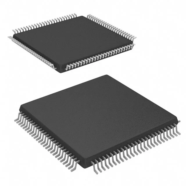
512Kbit dual-port asynchronous SRAM — 25 ns access, 5V supply
The CY7C027AV-25AXI: Operating from a 4.5V to 5.5V supply, this part sits in legacy 5V logic domains — it does not tolerate 3.3V or lower rails without a level translator, so a BOM carrying 3.3V FPGAs or MCUs needs a voltage translator on the address/data bus.
100-TQFP footprint and board integration
Housed in a 100-LQFP package with a 14x14 mm body (supplier device package 100-TQFP), this SRAM demands a fine-pitch soldering profile — the 0.5 mm lead pitch requires a stencil aperture designed for the specific paste height to avoid bridging on the inner rows, and a reflow profile that stays below 260°C peak to protect the die attach. The parallel interface connects directly to the system address and data buses without serialization latency — each read or write cycle completes in one 25 ns window, which is the key advantage over serial SRAM for applications needing deterministic access latency like video frame buffers or multi-processor mailboxes.