Dual-port SRAM for shared-memory arbitration
The CY7C026A-15AXC is a 256Kbit dual-port asynchronous SRAM organized as 16K x 16, with a 15 ns access time. Two independent ports allow simultaneous read/write from separate bus masters, making it a fit for shared-memory designs in telecom switches, video frame buffers, or multiprocessor systems where one memory bank serves two controllers without arbitration logic.
Speed grade and bus timing
The 15 ns access time and 15 ns write cycle time set the bus-speed ceiling for the port interface. At this speed, the part supports back-to-back read/write cycles at roughly 33 MHz — adequate for 8- or 16-bit microcontrollers with wait-state-free access, but not for high-throughput DSP pipelines that need sub-10 ns SRAM. The parallel memory interface uses standard asynchronous control signals (CE, OE, WE) on each port — no clock or refresh cycle, so the timing model is straightforward for FPGA or CPLD glue logic.
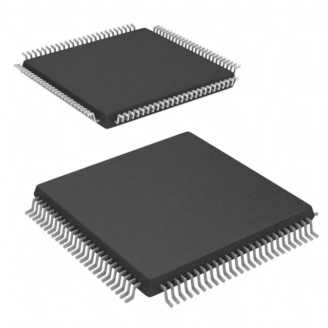
Supplied in a 100-LQFP (14x14 mm body) surface-mount package, the CY7C026A-15AXC uses a 0.5 mm pitch — a standard footprint that routes on a 4-layer board without micro-vias. The tray packaging means the parts arrive in anti-static trays, not tape-and-reel; plan for pick-and-place with a tray feeder or manual loading.
Because this is a discontinued dual-port SRAM with no pin-compatible replacement from Infineon, a board redesign may be required if the supply channel dries up. The 100-LQFP footprint is common across several dual-port SRAM vendors; a cross-reference search against IDT or Renesas parts with the same package and speed grade is a practical hedge.