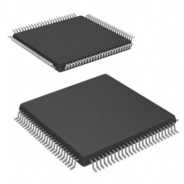
The CY7C0251-25AXC is listed as Obsolete by Infineon.
25 ns dual-port SRAM — what the speed grade means for bus timing
This is a 144Kbit dual-port asynchronous SRAM organized as 8K words by 18 bits. The 25 ns access time and 25 ns write cycle time set the minimum bus cycle — a master reading or writing this device must allow at least 25 ns from address valid to data valid (read) or from write enable to data latch (write). That puts the maximum sustainable bus rate around 40 MHz in a zero-wait-state system, though board-level trace delay and capacitive loading will reduce the practical ceiling. The dual-port architecture means two independent buses (address, data, and control) can access the memory array simultaneously. No external arbitration logic is needed for concurrent reads or writes to different addresses; simultaneous writes to the same address produce a contention condition that the system must avoid through software handshaking or a semaphore flag.
100-TQFP — rework and board-fit considerations
Housed in a 100-lead TQFP with a 14x14 mm body (supplier device package 100-TQFP). The tray packaging is standard for QFPs; pick-and-place lines need a tray feeder or a tube-to-tray conversion.