For sustainment of existing designs, the only channel is the independent distribution market — surplus, new-old-stock, or qualified broker inventory. Any replacement would require a form-fit-function evaluation of a different dual-port SRAM family or a redesign around a FIFO or shared-RAM architecture.
In a dual-port configuration where two independent buses (e.g., a DSP and an FPGA) share this memory, 25 ns sets the minimum bus cycle time for each port. If your system clock runs at 40 MHz (25 ns period), this part gives zero wait-state reads on both ports simultaneously — but only if the address hold and data setup margins are clean. At 50 MHz (20 ns period), you will need at least one wait state on one port.
128Kbit organized as 8K x 16 — sizing the buffer
The 128Kbit memory is organized as 8K words of 16 bits each. For a dual-port SRAM used as a shared mailbox between two processors, 8K words is enough for moderate-sized command queues or status tables.
84-PLCC J-Lead — legacy footprint, rework considerations
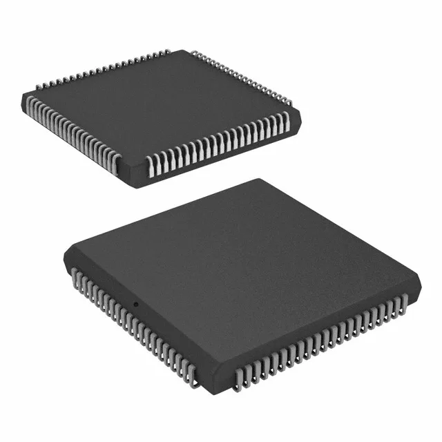
The 84-LCC (J-Lead) package body measures 29.31 mm square. J-Lead packages are less common in modern production lines than QFP or BGA; rework requires a hot-air nozzle sized for the PLCC body.
Supply and temperature — fit check
This is important: if your system runs on 3.3 V or lower, this part needs a separate 5 V rail or a level translator on the address/data buses. The part is surface-mount only, in the 84-PLCC package.