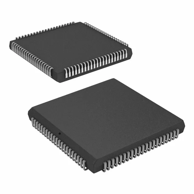
The Cypress CY7C025-25JC is a 128Kbit dual-port asynchronous SRAM organized as 8K x 16 bits. It gives two independent systems simultaneous read/write access to a common memory array through separate left and right ports, each with its own address, data, and control lines. The 25 ns access time sets the arbitration latency — both sides must respect the busy flag logic to avoid data corruption when addresses collide.
The 25 ns access time means the memory presents valid data within 25 ns of the address being stable on either port. In a dual-processor or FPGA-to-processor mailbox, this sets the minimum cycle time for back-to-back reads.
Cypress (now part of Infineon) no longer manufactures this device. For production builds or repair stock, the part must be sourced through independent distribution — surplus, new-old-stock, or qualified broker channels. The 84-PLCC package (29.31 mm x 29.31 mm) is a JEDEC footprint that some newer dual-port SRAMs share, but verify pin compatibility before substituting.
Supplied in a Tube, this surface-mount device uses an 84-lead PLCC with J-bend leads (84-LCC). The package body measures 29.31 mm per side. PLCC sockets are available for prototyping, but production boards typically solder directly. The J-lead footprint requires a reflow profile consistent with standard SnPb or Pb-free solders — no special thermal pad or exposed paddle.