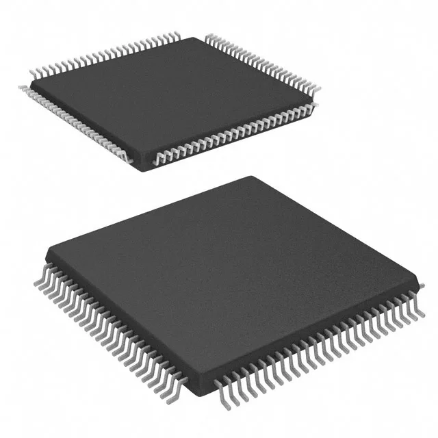
The Cypress CY7C025-25AXC is a 128 Kbit asynchronous dual-port SRAM organized as 8K words by 16 bits. It gives two independent systems — typically a DSP and an MCU, or two processor buses — simultaneous read/write access to a shared memory array without external arbitration logic. The 25 ns access time means each port can complete a read or write cycle in 25 ns, which supports bus speeds up to 40 MHz with zero wait states, assuming the bus-arbitration handshake is clean. It comes in a 100-lead TQFP (14x14 mm) package for surface-mount assembly.
For a system running a 40 MHz bus clock (25 ns period), this part can deliver data within a single clock edge-to-edge window, but setup and hold margins on the controller side will be tight — typically 2–3 ns of margin after accounting for PCB trace delay and output hold. If your controller's data setup requirement exceeds 3 ns, you may need to insert a wait state or drop to a slower clock. Write cycle time is also 25 ns, so the write pulse width must be at least that wide. The parallel interface (address, data, and control lines) means all signals must settle within that window — a common pitfall on boards with long traces or multiple loads.
Any replacement must be pin-compatible in the 100-TQFP footprint and match the 5 V supply, 25 ns timing, and 8K x 16 organization — a non-trivial search because most newer dual-port SRAMs have moved to 3.3 V or lower.
Dual-port architecture: the arbitration decision
This part uses asynchronous dual-port architecture with on-chip arbitration. Both ports have independent address, data, and control lines. When both ports address the same memory location simultaneously, the internal logic resolves the conflict based on which port's address strobe arrives first — the other port's cycle is held off via a BUSY flag. In a design review, confirm that both controllers can handle the BUSY handshake; some legacy DSPs lack a dedicated input for this.