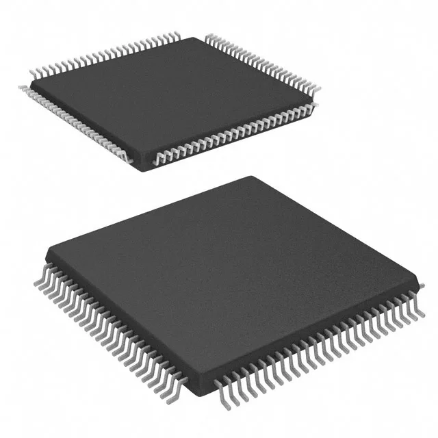
What this dual-port SRAM does
The Cypress CY7C025-15AXCT is a 128Kbit dual-port asynchronous SRAM organized as 8K words by 16 bits. Its two independent ports let two bus masters — two microcontrollers, a DSP and an FPGA, or a CPU and a DMA controller — read and write the same memory array without arbitration logic. Each port has its own chip enable, output enable, and write enable pins, plus separate address and data buses.
For a system running a 50 MHz bus (20 ns cycle), this part leaves 5 ns of margin for address setup, hold, and propagation delay through buffers or level shifters. At 66 MHz (15 ns cycle), the access time exactly matches the bus period, so zero-wait-state operation is possible only if the board layout keeps trace lengths short and the address-to-data path clean.
5V-only supply — plan for level translation
If your host processor runs at 3.3V or 1.8V, every address, data, and control pin on both ports needs bidirectional level translation. The 15 ns access time budget shrinks by the propagation delay of the translator, so choose a fast translator (sub-5 ns) to keep the bus margin intact.
Cypress lists the CY7C025-15AXCT as obsolete. No last-time-buy window remains open from the manufacturer. There is no pin-compatible direct replacement from Cypress (now Infineon) in the same dual-port family; the closest functional alternatives use different packages or supply voltages and require a board spin. If you need a drop-in substitute, verify the exact footprint and timing against the original design before committing.