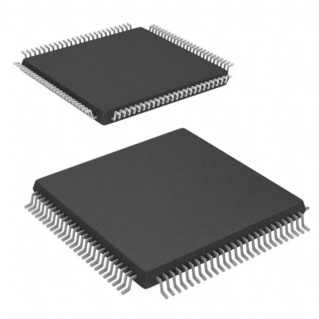
The CY7C025-15AXC is officially classified as Obsolete by Infineon. There is no listed successor in the official record, so new-production allocation is not available through the factory channel.
In a shared-memory system between two processors or a processor and an FPGA, that 15 ns window determines whether the address-to-data valid timing closes at the system clock rate. At 5V nominal, the propagation delays through the address and control buffers eat into that margin, so the board-level trace length and loading matter — the 15 ns is the datasheet maximum, not a typical. If your design runs at 33 MHz or faster, budget the full 15 ns plus derating for temperature and supply tolerance.
128Kbit organized 8K x 16 — buffer sizing
At 128Kbit total, organized as 8K words of 16 bits each, this part fits applications that need a moderate-sized shared mailbox or data buffer — for example, a 16-bit DSP passing blocks of coefficients to a host microcontroller, or a dual-processor intercommunication FIFO. The 16-bit wide data bus matches 16-bit MCUs and many FPGA soft-core buses without byte packing. If your design needs more than 8K words or a 32-bit data path, you would step up to a larger density in the same family, but the 100-pin TQFP footprint is the same across several Infineon dual-port SRAM options, so a board-level pin-compatible migration is possible within the family.
5V supply — legacy rail, not 3.3V
The supply range is 4.5V to 5.5V, which anchors this part in the 5V logic ecosystem. If your board runs a 3.3V core with a 5V peripheral bus, you will need level translation on the address, data, and control lines. The part is not rated for 3.3V operation — the minimum is 4.5V — so a direct drop-in to a 3.3V-only design will not work. This also means the I/O thresholds are TTL-compatible but not 3.3V CMOS, so check the Vih/Vil levels against your host controller.
It is not qualified for industrial or automotive temperature ranges. If your application sees -40°C or +85°C, you need the industrial-temperature variant (CY7C025-15AXI or similar) which shares the same footprint but carries a different ordering code.
Package and footprint — 100-TQFP 14x14
The shipping medium is Tray, not Tape & Reel, which matters if you use automated pick-and-place: verify that your feeder setup accepts trays, or plan a transfer to tape.