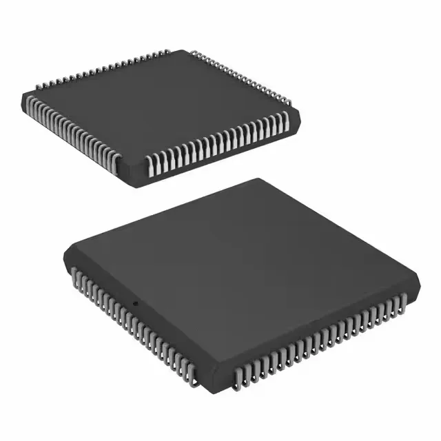
The Infineon (Cypress) CY7C024-55JXC is a 64Kbit dual-port asynchronous SRAM organized as 4K x 16 bits.
55 ns access time — timing margin in a shared-bus design
The 55 ns access time and 55 ns write cycle time set the bus timing budget. In a shared-memory system with two controllers running at 20 MHz (50 ns cycle), the 55 ns access means the SRAM is the speed-limiting element — the bus must insert a wait state or the controllers must stretch their read cycle. For 25 MHz (40 ns cycle) or faster buses, this part falls out of the timing budget entirely. The 55 ns figure is the same for both read access and write cycle, which simplifies the timing closure but leaves no margin for capacitive loading on long board traces.
84-PLCC J-Lead — rework and footprint considerations
Housed in an 84-lead PLCC with J-leads (29.31 mm square body), the package is surface-mount but through-hole-compatible in terms of rework — J-lead packages are socketable and relatively easy to remove with hot air without damaging the board. The 1.27 mm lead pitch is forgiving for manual inspection. No thermal pad, so all heat dissipates through the leads into the PCB copper; for continuous operation at 70°C ambient, ensure adequate copper area on the PLCC footprint's thermal land.
Cypress (now Infineon) no longer manufactures this specific variant. The only supply channel is the independent distribution market — brokers and excess-stock holders who still hold inventory from the last production runs. Date-code and quality verification become critical — PLCC packages are susceptible to moisture sensitivity, and parts sitting in inventory for years may need a bake before reflow. We source through vetted independent channels and confirm condition before quoting.