25 ns access and dual-port arbitration
The CY7C024-25AXI: The 25 ns access time means the memory completes a read or write cycle within that window from address assertion — critical when two processors or an FPGA and a CPU contend for the same memory space without a shared clock. The write cycle time, word and page, is also 25 ns, so the bus turnaround is symmetric. As a dual-port asynchronous SRAM, it provides two independent ports with separate address, data, and control lines. Each port can access any memory location simultaneously; the internal arbitration logic resolves contention when both ports target the same address, asserting a BUSY flag to the losing port.
100-TQFP package and board integration
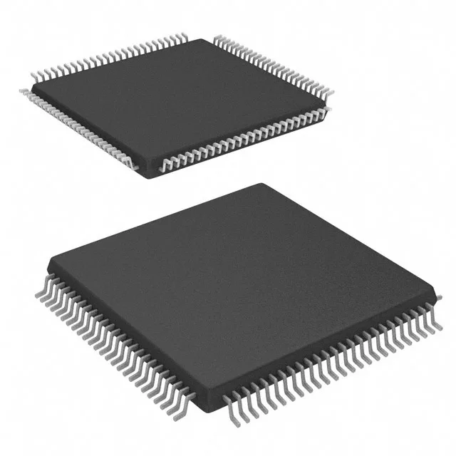
Housed in a 100-TQFP (14x14 mm) package, the CY7C024-25AXI is a surface-mount device. The 0.5 mm pitch demands careful PCB layout — a 4-layer board is typical for fan-out of the 100 pins, with decoupling capacitors placed close to each supply pair to maintain signal integrity at 25 ns edge rates.
Sourcing an obsolete dual-port SRAM
For new designs, consider a more recent dual-port SRAM family with a similar 4K x 16 organization and 5 V supply tolerance, though a board respin to a different package may be required.