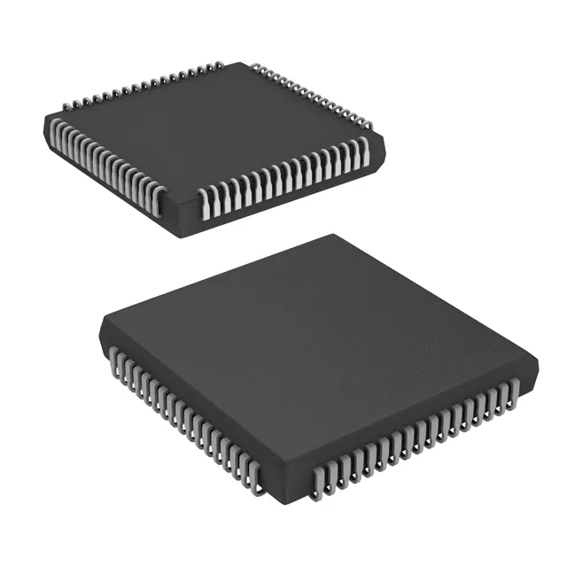
The Cypress CY7C006A-20JXCT is a 128Kbit (16K x 8) dual-port asynchronous SRAM that allows two independent processors or controllers to access a common memory array without bus contention. Its 20 ns access time sets the timing budget for read and write cycles in shared-memory designs, such as multiprocessor systems, network switches, or industrial controllers where a single memory buffer must be visible to two bus masters.
In a dual-port architecture, both ports share the same memory array, and arbitration logic resolves simultaneous accesses. The 20 ns figure sets the minimum cycle time for back-to-back reads or writes from either port, and it directly affects the hold-time margin on the data bus. For a system running a 50 MHz bus clock (20 ns period), this part leaves essentially zero margin for decode delays — it is best suited to slower buses or designs where the access time can be absorbed by wait states.
68-PLCC J-Lead — legacy footprint, rework considerations
Housed in a 68-lead PLCC with J-bend leads (68-PLCC, 24.23 mm x 24.23 mm body), this part is surface-mount but uses a J-Lead form factor common in 1990s–2000s designs. The PLCC socket is a known failure point in high-vibration environments; soldered direct is more reliable but requires a hot-air rework station for removal.
Cypress Semiconductor officially lists the CY7C006A-20JXCT as Obsolete. Buyers should expect date codes from past production lots and verify device authenticity through visual inspection and functional testing. There is no direct pin-compatible replacement from Cypress — the CY7C006 family has no active-production successor in the same 68-PLCC footprint. For new designs, consider a more modern dual-port SRAM in a BGA or QFP package, or evaluate a serial-memory approach with a dual-port bridge FPGA.