A 20 ns access time means the SRAM can complete a read or write cycle within 20 ns of the address being valid. The 20 ns write cycle time matches the read access, so back-to-back operations don't introduce a dead cycle on the bus.
Dual-port architecture — shared memory without arbitration logic
Dual-port SRAM integrates two independent address, data, and control ports on one die, so two bus masters can access the same 16K x 8 memory array without external arbitration logic. Each port has its own chip enable, output enable, and write enable pins. When both ports address the same memory location simultaneously, an internal arbiter resolves the collision — the CY7C006A-20JC uses a busy-flag handshake to stall the second port until the first completes.
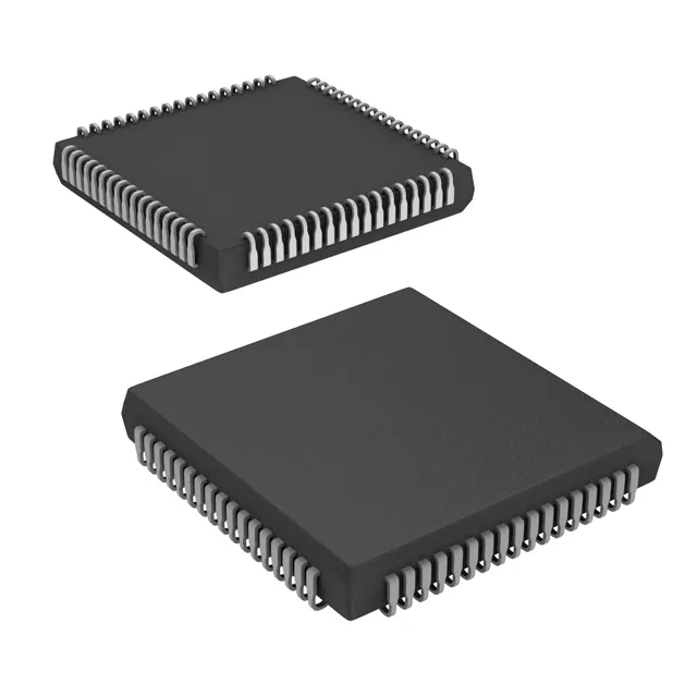
68-PLCC — footprint and handling
The 68-lead PLCC (J-lead) package measures 24.23 x 24.23 mm body size. J-leads are formed under the package body, so the footprint requires a PLCC socket or a solder-paste stencil with the correct J-bend land pattern.