PLL-based clock driver with 200 MHz LVTTL fanout
The CY7B9973V-AC is a PLL-based clock buffer from Infineon designed to distribute a clean LVTTL clock signal across multiple loads. It accepts one or two LVTTL inputs and provides up to 13 LVTTL outputs, with a maximum operating frequency of 200 MHz. The supply voltage range of 2.97V to 3.63V lets it run on a standard 3.3V rail with margin for ripple.
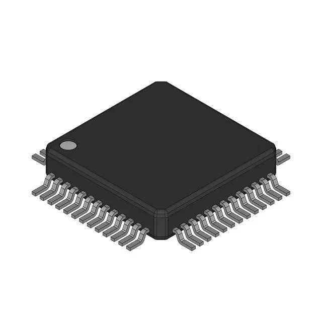
52-TQFP package and layout considerations
The input side accepts differential or single-ended LVTTL; the output side is single-ended LVTTL only. The 2:13 ratio means you can feed two independent clock sources and select between them, or use one input and leave the other grounded — the datasheet covers the logic thresholds.
Active production, RoHS non-compliant
The part is RoHS non-compliant (lead-bearing solder balls or die-attach), so it cannot ship into EU RoHS-required assemblies without an exemption. For RoHS-constrained BOMs, check the CY7B9973V-AC's lead-free variant or a pin-compatible alternative.