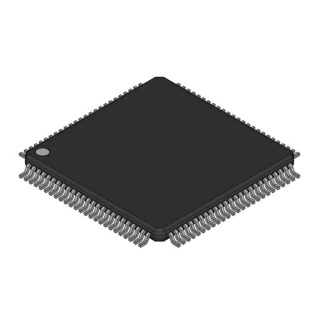
Infineon Technologies CY7B994V — Clock & Timing ICs

Cypress CY7B994V RoboClock™ Clock Buffer, 200 MHz

MPNCY7B994V
End of Life

Cypress RoboClock™ CY7B994V, PLL-based clock buffer and fanout distribution, 200 MHz max, 4:18 input:output ratio, LVPECL/LVTTL input, LVTTL output, 2.97V–3.63V supply, single circuit.

$34.0Ref. price · indicative, final on quote
StockContact for availability
MOQ1 pcs
  • 100% new & originalTraceable channels only — no refurbs, no pulls, no remarked parts.
  • Date & lot codes on quoteStated per line before you commit; label photos on request.
  • MSL-compliant ESD packingMoisture-sealed bags with indicator cards; reels photo-verified.
  • PayPal buyer protectionPay by T/T, PayPal or Payoneer — card payments covered end to end.

Specifications

CY7B994V Technical Specifications
ParameterValue
TypeClock Buffer, Fanout Distribution
SeriesRoboClock™
Voltage2.97V ~ 3.63V
Frequency200MHz
PLLYes
InputLVPECL, LVTTL
OutputLVTTL
PackageBulk
Divider (Multiplier)Yes/Yes
Number of circuits1
Ratio - Input:Output4:18
Differential - Input:OutputNo/No

Product details

What the CY7B994V is and where it fits

The Cypress CY7B994V is a PLL-based clock driver from the RoboClock™ family, configured as a clock buffer and fanout distribution device. It accepts up to four input clocks (LVPECL or LVTTL) and drives eighteen LVTTL outputs, all from a single 2.97 V to 3.63 V supply. The integrated PLL allows zero-delay synthesis and skew management, making this part suited for distributing a clean reference clock across multiple loads on a PCB — think telecom line cards, baseband processors, or FPGA banks that need a synchronous fanout without adding separate PLLs per lane.

200 MHz maximum — what it means for the bus

The 200 MHz ceiling sets the upper speed grade for the output clocks. At this frequency the part can drive synchronous interfaces like DDR memory reference clocks, gigabit Ethernet MAC/PHY timing, or high-speed ADC/DAC sample clocks. The 4:18 ratio is the headline number — eighteen outputs from four inputs means one chip replaces multiple smaller fanout buffers, saving board area and reducing part count. The divider/multiplier block gives the designer flexibility to synthesize different output frequencies from a single input, though the outputs are all LVTTL and non-differential, so this part is not for differential pairs like LVPECL or LVDS fanout.

Lifecycle and compliance reality

This part is RoHS non-compliant, meaning it uses lead-bearing solder or other restricted substances.

Frequently asked questions

Is CY7B994V RoHS compliant?

No, the CY7B994V is listed as RoHS non-compliant. It uses lead-bearing materials and cannot be used in RoHS-mandated assemblies without an exemption.

What is the maximum frequency of CY7B994V?

The maximum frequency is 200 MHz. This is the upper speed limit for the output clocks.

What is the input to output ratio of CY7B994V?

The ratio is 4 inputs to 18 outputs. Four clock inputs (LVPECL or LVTTL) can be fanned out to eighteen LVTTL outputs.

When sourcing CY7B994V, what is the closest functional second-source — CY2305SXI-1HT?

The CY2305SXI-1HT is a different part: it is a zero-delay buffer with a 1:5 fanout, 133.33 MHz max, and 3.0 V supply. It does not match the CY7B994V's 4:18 ratio, 200 MHz ceiling, or LVPECL input capability, so it is not a direct functional second-source for a high-fanout design.