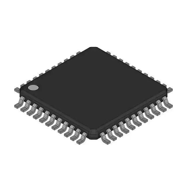
Infineon Technologies CY7B9940V-2AC — Clock & Timing ICs

CY7B9940V-2AC RoboClockII Junior PLL Clock Buffer, 200 MHz

MPNCY7B9940V-2AC
End of Life

Cypress RoboClockII™ Junior, PLL-based clock buffer/zero-delay buffer, 200 MHz max frequency, 4:10 input:output ratio, LVPECL/LVTTL input, LVTTL output, 2.97 V to 3.63 V supply, 44-TQFP, 0°C to 70°C.

$15.81Ref. price · indicative, final on quote
Packaging44-LQFP
StockContact for availability
MOQ1 pcs
  • 100% new & originalTraceable channels only — no refurbs, no pulls, no remarked parts.
  • Date & lot codes on quoteStated per line before you commit; label photos on request.
  • MSL-compliant ESD packingMoisture-sealed bags with indicator cards; reels photo-verified.
  • PayPal buyer protectionPay by T/T, PayPal or Payoneer — card payments covered end to end.

Specifications

CY7B9940V-2AC Technical Specifications
ParameterValue
TypeClock Buffer, Zero Delay Buffer
SeriesRoboClockII™ Junior
Mounting typeSurface Mount
Voltage2.97V ~ 3.63V
Frequency200MHz
Operating temperature0°C ~ 70°C (TA)
PLLYes
InputLVPECL, LVTTL
OutputLVTTL
PackageBulk
Case44-LQFP
Divider (Multiplier)Yes/No
Number of circuits1
Ratio - Input:Output4:10
Differential - Input:OutputYes/No

Product details

PLL-based clock distribution for 200 MHz trees

The Cypress CY7B9940V-2AC is a PLL-based clock buffer from the RoboClockII Junior family. It accepts LVPECL or LVTTL inputs and delivers LVTTL outputs across a 4:10 input-to-output ratio, with a maximum operating frequency of 200 MHz.

4:10 fanout — what it means for the clock tree

The 4:10 ratio means this buffer can accept up to four independent clock inputs and distribute them to ten outputs. In practice, that lets a designer fan out a single master clock to multiple destination ICs (FPGAs, PHYs, ASICs) while keeping skew low across the bank. The differential input (LVPECL) option is useful when the reference clock arrives over a twisted pair or a long board trace; the single-ended LVTTL input works for local on-board oscillators. All ten outputs are LVTTL, so the downstream logic must accept that logic level — no CML or HCSL on the output side.

Supply and temperature — deployment context

The supply range is 2.97 V to 3.63 V. The operating temperature range is 0°C to 70°C.

Lifecycle and sourcing reality

Note that this part is marked RoHS non-compliant, so it is not suitable for new designs requiring RoHS exemption-free assembly. For RoHS-compliant builds, a lead-free variant or a different buffer should be selected.

Frequently asked questions

What is the equivalent or replacement for CY7B9940V-2AC?

A functional peer is the CY2305SXI-1HT, also a zero-delay buffer, but with a 1:5 fanout ratio (vs 4:10), no differential input, and a maximum frequency of 133.33 MHz. The CY7B9940V-2AC offers higher fanout and differential input capability, so the CY2305 is not a direct pin-compatible substitute — it fits simpler, lower-speed clock trees.