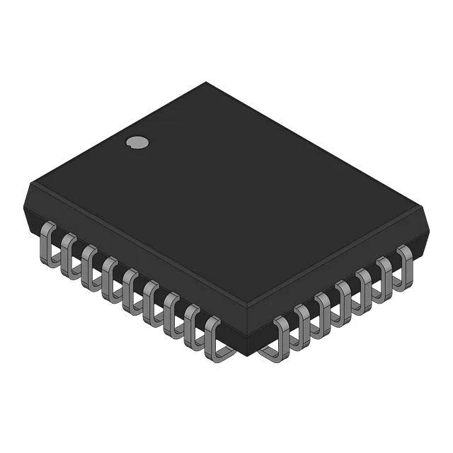
Infineon Technologies CY7B992-2JCT — Clock & Timing ICs

Cypress CY7B992-2JCT PLL Clock Driver, 80 MHz, 1:8 Fanout

MPNCY7B992-2JCT
End of Life

Cypress CY7B992-2JCT, PLL-based zero-delay fanout buffer, 80 MHz max frequency, 1:8 CMOS outputs, 5V supply, 32-PLCC (J-lead), commercial temperature.

$13.34Ref. price · indicative, final on quote
Packaging32-LCC (J-Lead)
StockContact for availability
MOQ1 pcs
  • 100% new & originalTraceable channels only — no refurbs, no pulls, no remarked parts.
  • Date & lot codes on quoteStated per line before you commit; label photos on request.
  • MSL-compliant ESD packingMoisture-sealed bags with indicator cards; reels photo-verified.
  • PayPal buyer protectionPay by T/T, PayPal or Payoneer — card payments covered end to end.

Specifications

CY7B992-2JCT Technical Specifications
ParameterValue
TypeFanout Buffer (Distribution), Zero Delay Buffer
Mounting typeSurface Mount
Voltage4.5V ~ 5.5V
Frequency80MHz
Operating temperature0°C ~ 70°C (TA)
PLLYes
InputCMOS
OutputCMOS
PackageBulk
Case32-LCC (J-Lead)
Divider (Multiplier)Yes/Yes
Number of circuits1
Ratio - Input:Output1:8
Differential - Input:OutputNo/No

Product details

PLL-based clock distribution — what it does

The CY7B992-2JCT is a PLL-based clock driver from Cypress that combines a zero-delay buffer with a 1:8 fanout. It takes a single CMOS input and regenerates eight CMOS outputs phase-aligned to the reference, with the PLL cleaning up jitter and skew. The part includes an internal divider and multiplier, so you can synthesize a different output frequency from the input — useful for generating a multiple of a reference clock without an external VCXO.

80 MHz ceiling and the 5V supply reality

Rated for 80 MHz maximum, the CY7B992-2JCT covers the common clock speeds for 100Base-T Ethernet, PCI, and mid-range processor buses. The supply range is 4.5V to 5.5V — a straight 5V part. It is not 3.3V tolerant on the input or output, so if your board runs a 3.3V clock tree you need a level translator or a different buffer. The 1:8 ratio means a single input drives eight loads, which saves a second buffer stage in a moderate fanout design.

Package and temperature — where it fits

Housed in a 32-PLCC with J-leads (11.43x13.97 mm body), the part is surface-mount but uses a PLCC footprint — not the same as a QFP or SOIC. The operating temperature range is 0°C to 70°C, which limits it to commercial indoor equipment: servers, telecom line cards, test gear, and office networking. Not rated for industrial or automotive environments.

Lifecycle and sourcing posture

It remains a current-production part, so the supply channel is the standard franchise distribution, not the surplus market. The part is RoHS non-compliant, which matters if your assembly line is restricted to lead-free solder; verify your reflow profile and exemption status before committing the BOM.

Frequently asked questions

Is the CY7B992-2JCT compatible with 3.3V logic?

No. The supply range is 4.5V to 5.5V and both input and output are CMOS at 5V levels. 3.3V logic will not reliably drive the input, and the outputs will exceed 3.3V receiver limits. A level translator is required if the rest of the board runs at 3.3V.