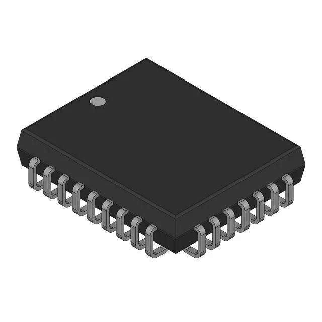
The Cypress CY7B9911V-7JC is a PLL-based zero delay buffer from the RoboClock+™ family, designed to distribute a single LVTTL clock input to eight LVTTL outputs with minimal skew. It integrates a phase-locked loop for frequency synthesis and deskew, and includes both a divider and multiplier path.
The 110 MHz maximum frequency sets the upper bound for the clock input you can feed this buffer. If your system runs a 100 MHz reference for a switch ASIC or a 66 MHz PCI bus, this part has headroom. The 1:8 input-to-output ratio means one incoming clock drives eight outputs — enough to feed a handful of FPGAs, PHYs, or processors without adding a second buffer stage. That saves board area and reduces part count on the BOM.
Supply and temperature — the operating envelope
The supply range of 2.97 V to 3.63 V covers a nominal 3.3 V rail with about ±10% tolerance, so it works on a standard 3.3 V power plane. If your application lives in a data centre, office, or lab bench, this is fine. For industrial or automotive environments, you would need the industrial-temperature variant (if one exists in the family).
Package and field-service angle
The CY7B9911V-7JC comes in a 32-lead PLCC with J-leads (32-PLCC, body 11.43 x 13.97 mm). That J-lead footprint is socket-friendly — you can drop this into a PLCC socket on the board, which is a real advantage if you are doing field repairs without a rework station. No hot air, no paste stencil; just pop the old one out and press the new one in. The orientation is obvious from the chamfered corner, so it is hard to get wrong even in a parking lot.
The RoHS compliance status is marked as non-compliant, so if your BOM requires lead-free assembly, you will need to check whether your reflow profile and reliability requirements accept a tin-lead finish or if you need a RoHS-compliant alternative. For legacy designs that already run a tin-lead process, this is not a problem.