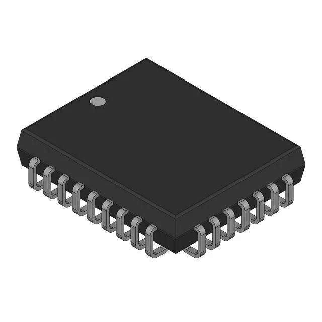
Infineon Technologies CY7B991-2JCT — Clock & Timing ICs

CY7B991-2JCT RoboClock PLL Clock Buffer, 80 MHz, 32-PLCC

MPNCY7B991-2JCT
End of Life

Cypress RoboClock™ series, CY7B991-2JCT, PLL-based Fanout Buffer (Distribution), Zero Delay Buffer, 1:8 ratio, 80 MHz max, CMOS I/O, 4.5V-5.5V supply, 32-PLCC (J-Lead), 0°C to 70°C.

$13.35Ref. price · indicative, final on quote
Packaging32-LCC (J-Lead)
StockContact for availability
MOQ1 pcs
  • 100% new & originalTraceable channels only — no refurbs, no pulls, no remarked parts.
  • Date & lot codes on quoteStated per line before you commit; label photos on request.
  • MSL-compliant ESD packingMoisture-sealed bags with indicator cards; reels photo-verified.
  • PayPal buyer protectionPay by T/T, PayPal or Payoneer — card payments covered end to end.

Specifications

CY7B991-2JCT Technical Specifications
ParameterValue
TypeFanout Buffer (Distribution), Zero Delay Buffer
SeriesRoboClock™
Mounting typeSurface Mount
Voltage4.5V ~ 5.5V
Frequency80MHz
Operating temperature0°C ~ 70°C (TA)
PLLYes
InputCMOS
OutputCMOS
PackageBulk
Case32-LCC (J-Lead)
Divider (Multiplier)Yes/No
Number of circuits1
Ratio - Input:Output1:8
Differential - Input:OutputNo/No

Product details

PLL clock distribution in a 32-PLCC package

The Cypress CY7B991-2JCT is a PLL-based clock buffer from the RoboClock series, combining fanout distribution and zero-delay buffering in a 32-lead PLCC package. It accepts one CMOS input and delivers eight CMOS outputs, with a maximum operating frequency of 80 MHz. The internal PLL aligns output edges to the input, eliminating propagation delay across the clock tree — useful for synchronising multiple loads on a single board.

5V supply and commercial temperature range

Operating temperature is rated 0°C to 70°C, which covers office equipment, telecom racks, and consumer electronics, but not industrial or automotive environments. The single-circuit design handles one PLL domain; for multiple independent clock domains you would need additional instances.

Active lifecycle — no obsolescence concern

No last-time-buy window is in effect. The part is RoHS non-compliant, so verify your assembly line's solder alloy compatibility if you are migrating to lead-free.

Rework and footprint notes

The 32-lead PLCC package uses J-leads, which are hand-reworkable with a hot-air station — the leads are visible and accessible. The body measures 11.43 x 13.97 mm. This footprint is not compatible with SOIC or QFP patterns, so a dedicated PLCC socket or land pattern is required.

Frequently asked questions

What are the direct alternatives or replacements for CY7B991-2JCT?

The CY2305SXI-1HT is a functional peer — also a PLL-based fanout buffer, but with a 1:5 output ratio, 3.3V supply, and industrial temperature range (-40°C to 85°C). The CY7B991-2JCT offers 1:8 outputs at 5V with commercial temperature; the CY2305SXI-1HT is not a pin-for-pin replacement but covers a similar role in 3.3V systems.

Can CY7B991-2JCT be used in 5V applications?

Yes, the supply range of 4.5V to 5.5V makes it suitable for 5V logic systems. Input and output are CMOS levels referenced to that supply rail.

What is the typical lead time for CY7B991-2JCT?

Lead time is confirmed at quote time against an RFQ. As an active part, it is generally available through distribution channels, but current lead times vary with demand and inventory.