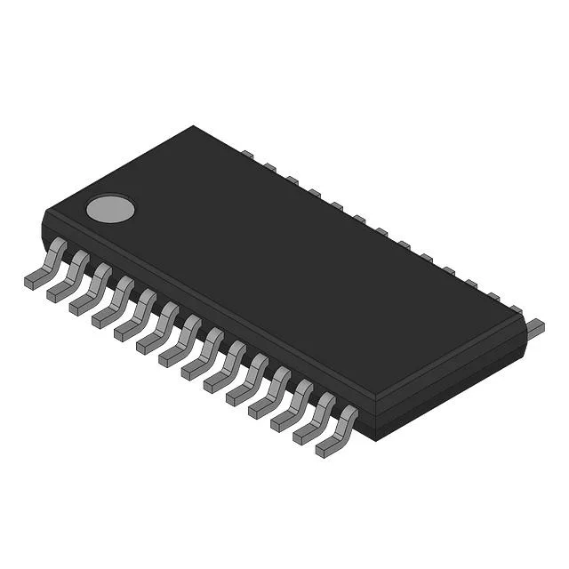
70 ns access time — timing margin for slower buses
For a microcontroller or FPGA running a parallel memory interface at moderate clock speeds, this provides comfortable timing margin without needing fast-page or synchronous modes.
RoHS non-compliance — a sourcing constraint
For designs targeting EU RoHS or similar environmental directives, this is a showstopper unless an exemption applies. If your project needs a RoHS-compliant 256Kbit asynchronous SRAM in the same footprint, consider the CY7C1399BN-12VXI family — though that part runs at 12 ns access and 3.0V nominal, so verify timing and supply margin before substituting.
No immediate LTB risk given its active status, but the RoHS restriction means supply may tighten as OEMs shift to compliant alternatives. For dual-sourcing resilience, the CY7C1399BN-12VXI is a functional peer in the same 32K x 8 organisation, though at a faster 12 ns access and 3.0V nominal supply — check your bus timing and voltage margin before qualifying it as a drop-in.