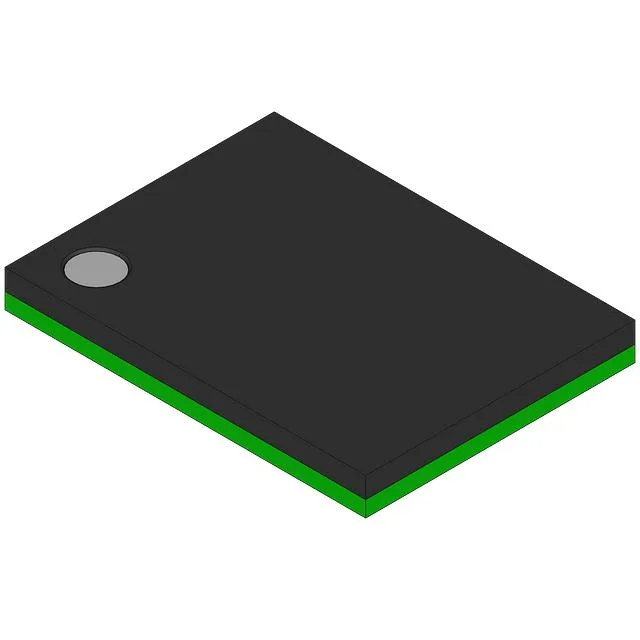
The CY62158DV30L-55BVI: The 55 ns access time defines the bus timing margin for the host controller. The parallel interface uses address, data, chip enable, output enable, and write enable signals.
Supply range and 3.3 V system fit
It also tolerates a 2.5 V supply, so it can bridge a mixed-voltage design without a level shifter on the memory bus — the I/O tracks Vdd.
Industrial temperature and deployment environments
No derating needed at the upper end; the 55 ns timing holds across the full temperature window.
Package: 48-VFBGA (6x8 mm)
Housed in a 48-ball VFBGA measuring 6x8 mm, this part saves about 40% board area versus a 44-pin TSOP. No exposed pad — all dissipation is through the balls into the PCB copper. The supplier device package code is 48-VFBGA (6x8).
Listed as Active by the manufacturer.