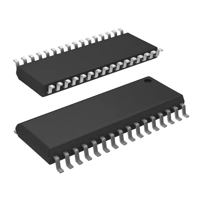
Infineon Technologies CY62148EV30LL-55SXI — Logic ICs

CY62148EV30LL-55SXI Infineon MoBL SRAM, 4Mbit, 55 ns

MPNCY62148EV30LL-55SXI
End of Life

Infineon MoBL CY62148EV30LL-55SXI, 4Mbit (512K x 8) asynchronous SRAM, 55 ns access time, 2.2V to 3.6V supply, parallel interface, -40°C to 85°C, 32-SOIC package.

$6.24Ref. price · indicative, final on quote
Packaging32-SOIC (0.445", 11.30mm Width)
StockContact for availability
MOQ1 pcs
  • 100% new & originalTraceable channels only — no refurbs, no pulls, no remarked parts.
  • Date & lot codes on quoteStated per line before you commit; label photos on request.
  • MSL-compliant ESD packingMoisture-sealed bags with indicator cards; reels photo-verified.
  • PayPal buyer protectionPay by T/T, PayPal or Payoneer — card payments covered end to end.

Specifications

CY62148EV30LL-55SXI Technical Specifications
ParameterValue
SeriesMoBL®
Memory typeVolatile
Mounting typeSurface Mount
Voltage2.2V ~ 3.6V
Memory interfaceParallel
Operating temperature-40°C ~ 85°C (TA)
PackageTube
TechnologySRAM - Asynchronous
Access time55 ns
Memory size4Mbit
Memory formatSRAM
Case32-SOIC (0.445\", 11.30mm Width)
Memory organization512K x 8
Write cycle time - word, page55ns

Product details

What this 4Mbit asynchronous SRAM brings to the bus

The Infineon CY62148EV30LL-55SXI is a 4Mbit (512K x 8) asynchronous SRAM from the MoBL® series, built for low-power standby in battery-backed and industrial designs. Its 55 ns access time sets the read-cycle floor — a 18 MHz bus can grab a word every cycle without wait states, but a 40 MHz MCU will need one wait inserted. The wide 2.2V to 3.6V supply range lets it sit on a 3.3V rail directly, no level translation on the address or data lines.

55 ns access — budget it against your processor clock

At 55 ns, this part is in the middle-speed tier for 4Mbit asynchronous SRAM. A 20 MHz bus cycle is 50 ns, so a back-to-back read requires one wait state. For a 16 MHz microcontroller the access fits within a single 62.5 ns cycle, yielding zero-wait performance. If your processor runs at 40 MHz or above, consider a 10 ns part like the CY7C1049GN30-10VXI — though that trades standby current for speed.

Package and footprint — the 32-SOIC wide body

The 32-SOIC package (0.445-inch body width, 11.30 mm) is a standard JEDEC outline for 512Kx8 asynchronous SRAM. The footprint is shared across several Infineon and legacy Cypress parts, so a board laid out for this package can also accept the CY7C1049GN30-10VXI if a speed upgrade is needed. Surface-mount assembly with standard reflow profile; MSL rating is typical for this package class — bake before reflow if the moisture-barrier bag has been open past the floor-life window.

3.3V logic compatibility — no level shifters needed

With a supply range of 2.2V to 3.6V, this SRAM operates directly from a 3.3V rail. All inputs and I/O are 3.3V-tolerant at that supply, so an MCU or FPGA with 3.3V CMOS outputs connects straight to the address and data bus without external level translators. The part also runs at 2.5V or 2.2V for battery-backed operation, though access time may stretch slightly at the low end of the range.

Frequently asked questions

What is the access time of CY62148EV30LL-55SXI?

The access time is 55 ns for both read and write cycles. This determines the maximum bus speed without wait states — a 16 MHz processor can run zero-wait, while a 40 MHz processor will need one wait state inserted.

Is CY62148EV30LL-55SXI compatible with 3.3V logic?

Yes. With a supply range of 2.2V to 3.6V, the part operates directly on a 3.3V rail. All inputs and I/O are 3.3V-tolerant at that supply, so no level shifters are needed between this SRAM and a 3.3V MCU or FPGA.