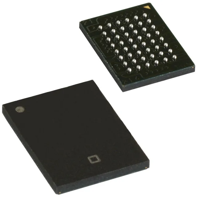
Infineon Technologies CY62147EV18LL-55BVXI — Discrete Semiconductors

Infineon CY62147EV18LL-55BVXI SRAM, 4Mbit, 55ns, 48-VFBGA

MPNCY62147EV18LL-55BVXI
End of Life

Infineon Technologies MoBL® series SRAM - Asynchronous, 4Mbit, 256K x 16, 55 ns access time, Parallel interface, 1.65V ~ 2.25V supply, -40°C ~ 85°C, 48-VFBGA (6x8), Bulk package.

$6.8Ref. price · indicative, final on quote
Packaging48-VFBGA
StockContact for availability
Lead timeIn Stock wk
MOQ1 pcs
  • 100% new & originalTraceable channels only — no refurbs, no pulls, no remarked parts.
  • Date & lot codes on quoteStated per line before you commit; label photos on request.
  • MSL-compliant ESD packingMoisture-sealed bags with indicator cards; reels photo-verified.
  • PayPal buyer protectionPay by T/T, PayPal or Payoneer — card payments covered end to end.

Specifications

CY62147EV18LL-55BVXI Technical Specifications
ParameterValue
SeriesMoBL®
Memory typeVolatile
Mounting typeSurface Mount
Voltage1.65V ~ 2.25V
Memory interfaceParallel
Operating temperature-40°C ~ 85°C (TA)
PackageBulk
TechnologySRAM - Asynchronous
Access time55 ns
Memory size4Mbit
Memory formatSRAM
Case48-VFBGA
Memory organization256K x 16
Write cycle time - word, page55ns

Product details

4 Mbit async SRAM in a 48-ball BGA

The CY62147EV18LL-55BVXI is a 4 Mbit asynchronous SRAM from Infineon's MoBL® series, organized as 256K x 16 bits. It runs on a 1.65 V to 2.25 V supply rail and delivers a 55 ns access time — fast enough for cache or working memory in embedded systems that don't need the complexity of a synchronous interface. It's a surface-mount part — not something you swap in the field without a hot-air station and a steady hand.

Supply and temperature envelope

The 1.65 V to 2.25 V supply range lets this SRAM work with 1.8 V logic families directly, without a level shifter on the address and data lines.

Board integration notes

The 48-VFBGA (6x8 mm) package has a 0.5 mm ball pitch — typical for this density. The supplier device package is 48-VFBGA (6x8), so the footprint matches the standard JEDEC outline for 48-ball BGA SRAMs. Write cycle time matches the read access at 55 ns — no penalty for mixed read/write patterns. The parallel interface is straightforward: CE#, OE#, WE# control, with byte-select for the upper and lower byte lanes on the 16-bit bus.

Frequently asked questions

What is the memory organization and access time of this SRAM?

It's organized as 256K x 16 bits (4 Mbit total) with a 55 ns access time. Both read and write cycle times are 55 ns, so it's symmetric for random access patterns.

What package does CY62147EV18LL-55BVXI use and is it field-replaceable?

It's in a 48-VFBGA (6x8 mm) package with 0.5 mm ball pitch. This is a surface-mount BGA — not socketed and not field-swappable without reflow equipment. Plan for PCB-level rework if a replacement is needed.