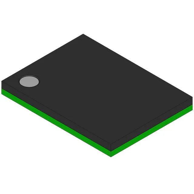
70 ns asynchronous SRAM — 2 Mbit in a 48-VFBGA
The CY62137CV30LL-70BVI: The parallel interface eliminates clock-tree complexity — address-to-data valid within 70 ns, no setup/hold on a clock edge. This part is built for industrial embedded systems, motor drives, and telecom line cards that need fast scratchpad or packet buffer memory without the overhead of synchronous SRAM or the endurance limits of flash.
48-VFBGA (6x8) — footprint and rework
The 48-VFBGA (6x8) package is a fine-pitch BGA with a 6 mm x 8 mm body. The ball pitch is 0.75 mm typical for this footprint — that drives via-in-pad or microvia fanout on the PCB. Reflow profile per J-STD-020; Hot-air rework is possible with a preheat plate and a fine-nozzle station, but expect to reball if the part has been through thermal cycles.
The 70 ns access time is guaranteed across the full temperature and supply range — no speed derating needed at the cold end.
That means no last-time-buy notice in effect, and the part is still in regular production.