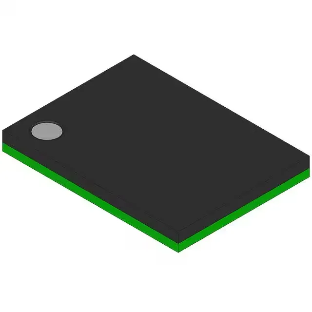
Infineon Technologies CY62137BV18LL-70BAI — Logic ICs

CY62137BV18LL-70BAI MoBL2 2Mbit Async SRAM, 70 ns, 1.8 V

MPNCY62137BV18LL-70BAI
End of Life

Infineon (Cypress) MoBL2™ CY62137BV18LL-70BAI, 2Mbit asynchronous SRAM, 128K x 16, 70 ns access, 1.75 V – 1.95 V supply, parallel interface, -40°C to 85°C, 48-TFBGA.

$3.2Ref. price · indicative, final on quote
Packaging48-TFBGA
StockContact for availability
MOQ1 pcs
  • 100% new & originalTraceable channels only — no refurbs, no pulls, no remarked parts.
  • Date & lot codes on quoteStated per line before you commit; label photos on request.
  • MSL-compliant ESD packingMoisture-sealed bags with indicator cards; reels photo-verified.
  • PayPal buyer protectionPay by T/T, PayPal or Payoneer — card payments covered end to end.

Specifications

CY62137BV18LL-70BAI Technical Specifications
ParameterValue
SeriesMoBL2™
Memory typeVolatile
Mounting typeSurface Mount
Voltage1.75V ~ 1.95V
Memory interfaceParallel
Operating temperature-40°C ~ 85°C (TA)
PackageBulk
TechnologySRAM - Asynchronous
Access time70 ns
Memory size2Mbit
Memory formatSRAM
Case48-TFBGA
Memory organization128K x 16
Write cycle time - word, page70ns

Product details

70 ns asynchronous SRAM for low-voltage, industrial-temperature designs

The Infineon (Cypress) CY62137BV18LL-70BAI is a 2Mbit asynchronous SRAM from the MoBL2™ family, organized as 128K x 16 bits. The parallel interface and 70 ns write cycle time make it a fit for legacy 16-bit microcontroller buses or low-power FPGA configuration stores that need a simple, no-clock SRAM at 1.8 V.

The 1.75 V to 1.95 V supply range is the first fit gate. If your board already has a 1.8 V rail (common in low-power MCU and FPGA designs), this SRAM connects directly. For 3.3 V or 2.5 V systems, you will need a level translator on the address and data lines, which adds cost and board area. The narrow tolerance also means the rail must be regulated — a 1.8 V LDO with ±2% accuracy keeps the SRAM inside its operating window.

70 ns access time — timing margin on a slow bus

For a microcontroller running at 10–20 MHz with a 50–100 ns bus cycle, this part provides adequate setup margin without wait states. It is not suited for high-speed DSP or cache applications where 10–15 ns synchronous SRAMs are the norm. The 70 ns write cycle time (word or page mode) matches the read timing, so back-to-back read-write sequences are straightforward.

48-FBGA footprint and assembly notes

The part comes in a 48-ball TFBGA (7x7 mm) package — a fine-pitch BGA that requires solder-paste stencil design, reflow profiling, and X-ray inspection after assembly. It is not hand-solderable in a rework loop. The 0.5 mm ball pitch demands careful PCB routing; fan-out vias are typically needed on inner rows.

Industrial temperature grade and deployment

The 1.8 V core keeps dynamic power low, which helps in convection-cooled enclosures.

Lifecycle and sourcing posture

It is RoHS non-compliant per the listing, so verify your assembly's exemption requirements if you are in a RoHS-regulated region.

Frequently asked questions

What is the access time of CY62137BV18LL-70BAI?

70 ns access time and 70 ns write cycle time (word/page).