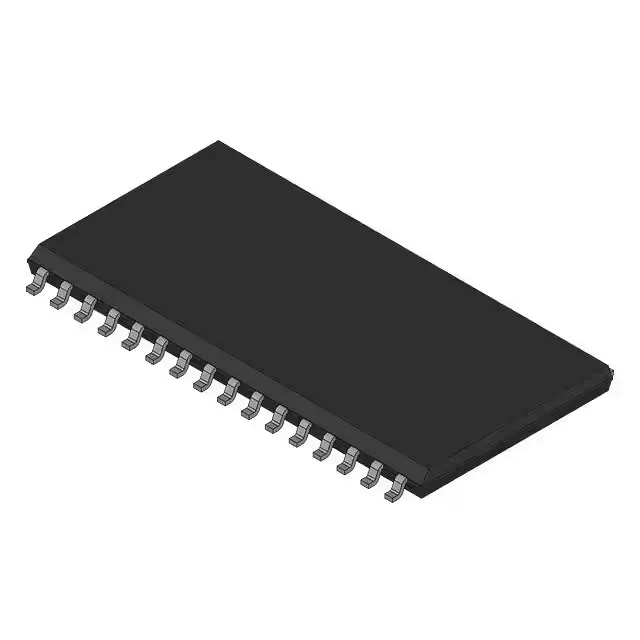
Infineon Technologies CY62128DV30L-70SI — Analog & Data Acquisition

CY62128DV30L-70SI Infineon MoBL SRAM, 1 Mbit, 70 ns

MPNCY62128DV30L-70SI
End of Life

Infineon MoBL® CY62128DV30L-70SI, 1 Mbit asynchronous SRAM, 128K x 8 organization, 70 ns access time, 2.2 V to 3.6 V supply, parallel interface, -40°C to 85°C, 32-SOIC.

$1.87Ref. price · indicative, final on quote
Packaging32-SOIC (0.445", 11.30mm Width)
StockContact for availability
MOQ1 pcs
  • 100% new & originalTraceable channels only — no refurbs, no pulls, no remarked parts.
  • Date & lot codes on quoteStated per line before you commit; label photos on request.
  • MSL-compliant ESD packingMoisture-sealed bags with indicator cards; reels photo-verified.
  • PayPal buyer protectionPay by T/T, PayPal or Payoneer — card payments covered end to end.

Specifications

CY62128DV30L-70SI Technical Specifications
ParameterValue
SeriesMoBL®
Memory typeVolatile
Mounting typeSurface Mount
Voltage2.2V ~ 3.6V
Memory interfaceParallel
Operating temperature-40°C ~ 85°C (TA)
PackageBulk
TechnologySRAM - Asynchronous
Access time70 ns
Memory size1Mbit
Memory formatSRAM
Case32-SOIC (0.445\", 11.30mm Width)
Memory organization128K x 8
Write cycle time - word, page70ns

Product details

MoBL 1 Mbit async SRAM — 70 ns access, byte-wide bus, industrial temp

The Infineon CY62128DV30L-70SI is a 1 Mbit asynchronous SRAM from the MoBL® series, organized as 128K x 8 bits with a 70 ns access time. It operates from a 2.2 V to 3.6 V supply and communicates over a parallel interface. The part is rated for -40°C to 85°C, making it suitable for industrial control, outdoor telecom, and factory automation where the memory bus needs deterministic read-write timing without refresh overhead.

70 ns access — what it means for bus timing

The 70 ns access time defines the window from address valid to data valid on a read cycle. The 70 ns write cycle time is symmetrical, so the bus timing budget is the same for both read and write operations.

128K x 8 organization — byte-wide fit

The 128K x 8 organization presents an 8-bit data bus. This directly matches 8-bit MCUs and DSPs without external byte-lane steering logic.

Industrial temperature range and package

The -40°C to 85°C operating range qualifies the part for environments where the enclosure sees outdoor temperature swings, such as base stations, solar inverters, and motor drives. The 32-SOIC (0.445" body width) is a surface-mount footprint common in industrial PCBs; it is not a fine-pitch BGA, so hand rework and inspection are straightforward.

RoHS non-compliant — legacy solder finish

This part is marked RoHS non-compliant, meaning the terminations use a tin-lead (SnPb) finish. It cannot be used in a lead-free reflow process without a RoHS exemption or waiver. For new designs requiring RoHS compliance, a lead-free variant from the MoBL family should be selected. For legacy production lines that still run SnPb solder, this part is a direct fit.

Active lifecycle — no LTB pressure

The CY62128DV30L-70SI carries an Active lifecycle status from Infineon (Cypress). There is no last-time-buy notice, no NRND flag, and no announced end-of-life.

Frequently asked questions

Is CY62128DV30L-70SI RoHS compliant?

No, the CY62128DV30L-70SI is listed as RoHS non-compliant. The terminations use a tin-lead (SnPb) finish, so it is not suitable for lead-free reflow processes without a RoHS exemption.

What is the access time of CY62128DV30L-70SI?

The access time is 70 ns for both read and write cycles. This is the time from address valid to data valid on a read, and the minimum write pulse width on a write.

What is the closest functional second-source for CY62128DV30L-70SI?

The CY7C1018DV33-10VXI is a 1 Mbit (128K x 8) asynchronous SRAM in the same 32-SOIC footprint with a 10 ns access time and 3.0 V supply. It is a faster alternative, but verify pin-compatibility and the supply voltage tolerance before substituting.