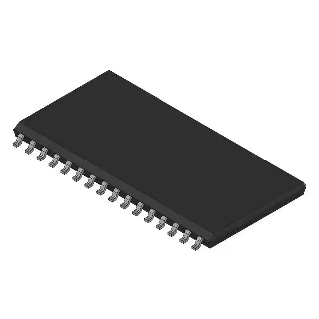
Infineon Technologies CY62128BNLL-70SI — Discrete Semiconductors

Infineon CY62128BNLL-70SI MoBL SRAM, 1Mbit, 70 ns, 32-SOIC

MPNCY62128BNLL-70SI
End of Life

Infineon Technologies MoBL® series, SRAM - Asynchronous, 1Mbit (128K x 8), Parallel interface, 70 ns access time, 4.5V ~ 5.5V, -40°C ~ 85°C, Surface Mount, 32-SOIC (0.445", 11.30mm Width), Bulk.

$1.11Ref. price · indicative, final on quote
Packaging32-SOIC (0.445", 11.30mm Width)
StockContact for availability
Lead timeIn Stock wk
MOQ1 pcs
  • 100% new & originalTraceable channels only — no refurbs, no pulls, no remarked parts.
  • Date & lot codes on quoteStated per line before you commit; label photos on request.
  • MSL-compliant ESD packingMoisture-sealed bags with indicator cards; reels photo-verified.
  • PayPal buyer protectionPay by T/T, PayPal or Payoneer — card payments covered end to end.

Specifications

CY62128BNLL-70SI Technical Specifications
ParameterValue
SeriesMoBL®
Memory typeVolatile
Mounting typeSurface Mount
Voltage4.5V ~ 5.5V
Memory interfaceParallel
Operating temperature-40°C ~ 85°C (TA)
PackageBulk
TechnologySRAM - Asynchronous
Access time70 ns
Memory size1Mbit
Memory formatSRAM
Case32-SOIC (0.445\", 11.30mm Width)
Memory organization128K x 8
Write cycle time - word, page70ns

Product details

70 ns access time and the read-cycle ceiling

The CY62128BNLL-70SI: The 70 ns access time sets the fastest read cycle the processor can request — at a 10 MHz bus clock (100 ns period), a single read fits within one cycle with 30 ns of margin for address decode and output settle; at 14 MHz (71 ns period), the margin disappears and the bus must insert a wait state. Write cycle time is also 70 ns, so the same timing budget applies to write operations — the word and page write modes share this ceiling, meaning a page-mode burst does not accelerate the write cycle itself, only the address sequencing between writes.

128K x 8 organization and the 5 V supply rail

Organised as 128K words of 8 bits, the CY62128BNLL-70SI presents a byte-wide data bus — it maps directly to an 8-bit microcontroller or a discrete address/data bus without byte-lane steering logic.

Industrial temperature grade and the 32-SOIC footprint

Housed in a 32-SOIC wide-body package (0.445-inch body width, 11.30 mm), the footprint is the standard JEDEC 300-mil SOIC-32 — the same pad pattern used by legacy 32-pin SRAMs and EEPROMs, so a board already routed for a 32-SOIC memory accepts this part without a layout change.

Active lifecycle and the RoHS flag

The part is marked RoHS non-compliant, meaning the lead-frame finish or mould compound contains lead above the RoHS exemption thresholds — if your assembly line or end-customer requires full RoHS compliance (e.g. for EU market or green-label products), this part does not meet that requirement and a Pb-free variant should be sourced.

Frequently asked questions

What package does the CY62128BNLL-70SI come in?

It is supplied in a 32-SOIC wide-body package (0.445-inch body width, 11.30 mm), surface-mount, with the supplier device package designation 32-SOIC. The footprint matches the standard JEDEC 300-mil SOIC-32 pattern.

Is the CY62128BNLL-70SI RoHS compliant?

No, Infineon lists this part as RoHS non-compliant. The lead-frame or mould compound contains lead above the RoHS exemption thresholds. A Pb-free variant should be sourced if full RoHS compliance is required.

How can I order the CY62128BNLL-70SI or check availability?

The CY62128BNLL-70SI is sourced to order against your BOM quantity through independent distribution.