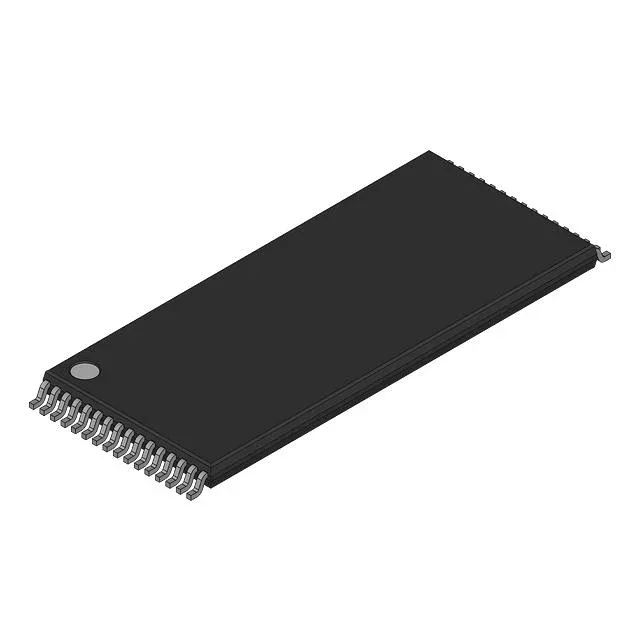
Infineon Technologies CY62128BLL-55ZRIT — Discrete Semiconductors

Infineon CY62128BLL-55ZRIT SRAM, 1Mbit, 55ns, 32-RTSOP

MPNCY62128BLL-55ZRIT
End of Life

Infineon Technologies MoBL® asynchronous SRAM, CY62128BLL-55ZRIT, 1Mbit (128K x 8), 55 ns access time, 4.5V-5.5V supply, -40°C to +85°C, 32-RTSOP package, Bulk.

$1.64Ref. price · indicative, final on quote
Packaging32-TFSOP (0.724", 18.40mm Width)
StockContact for availability
Lead timeIn Stock wk
MOQ1 pcs
  • 100% new & originalTraceable channels only — no refurbs, no pulls, no remarked parts.
  • Date & lot codes on quoteStated per line before you commit; label photos on request.
  • MSL-compliant ESD packingMoisture-sealed bags with indicator cards; reels photo-verified.
  • PayPal buyer protectionPay by T/T, PayPal or Payoneer — card payments covered end to end.

Specifications

CY62128BLL-55ZRIT Technical Specifications
ParameterValue
SeriesMoBL®
Memory typeVolatile
Mounting typeSurface Mount
Voltage4.5V ~ 5.5V
Memory interfaceParallel
Operating temperature-40°C ~ 85°C (TA)
PackageBulk
TechnologySRAM - Asynchronous
Access time55 ns
Memory size1Mbit
Memory formatSRAM
Case32-TFSOP (0.724\", 18.40mm Width)
Memory organization128K x 8
Write cycle time - word, page55ns

Product details

1 Mbit parallel SRAM for 5 V legacy buses

The CY62128BLL-55ZRIT is a 1 Mbit asynchronous SRAM from Infineon's MoBL® series, organized as 128K x 8 bits with a 55 ns access time.

55 ns access and 5 V supply — what they mean for the bus

The 55 ns access time sets the read-cycle floor: the processor must stretch its bus wait states to accommodate this window. On a 20 MHz bus (50 ns cycle), one wait state covers the access; at 25 MHz (40 ns cycle), two wait states are needed unless the memory controller supports a variable latency. The part draws its specified standby and active current at the nominal 5 V level; a drop to 4.5 V increases access time slightly but stays within the 55 ns max over the full temperature range. Asynchronous interface means no clock is needed — the chip select and output enable gates the data onto the bus directly. This simplifies the PCB layout compared to synchronous SRAM, but the address hold time relative to chip select must still meet the 55 ns write-cycle spec.

The 0.50 mm pin pitch and exposed pad require a solder-paste stencil aperture sized per the datasheet land pattern to avoid bridging during reflow.

Frequently asked questions

Can CY62128BLL-55ZRIT be replaced with CY62128BLL-55ZI?

Confirm the package and temperature grade against the BOM before substituting.

What is the memory organization of CY62128BLL-55ZRIT?

Organized as 128K words by 8 bits (128K x 8), giving a total of 1 Mbit of storage.