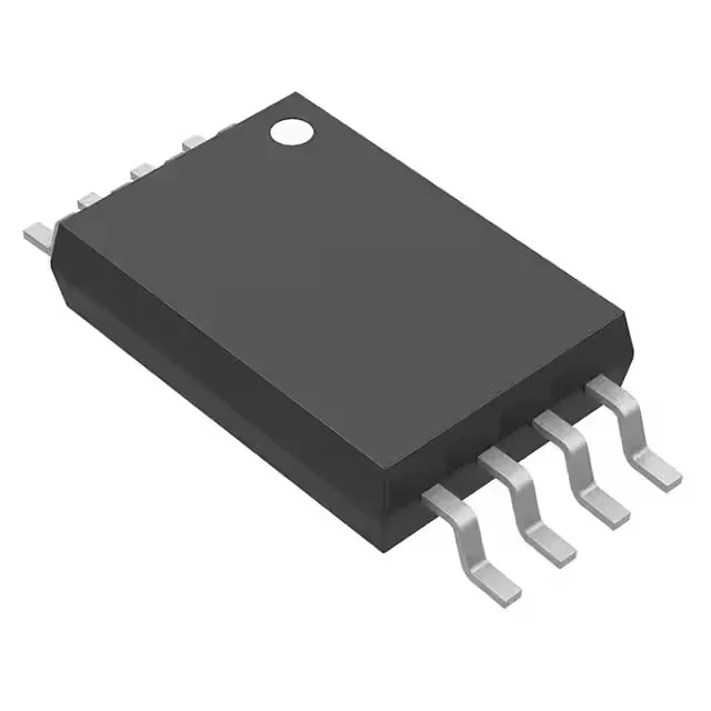
Infineon Technologies CY2XL12ZXI02 — Clock & Timing ICs

CY2XL12ZXI02 Clock Generator, PLL, 100 MHz LVDS, 8-TSSOP

MPNCY2XL12ZXI02
End of Life

Cypress CY2XL12ZXI02, Clock Generator, PLL Yes, Input CMOS/Crystal, Output LVDS, 100 MHz max, 1:1 ratio, 8-TSSOP, -40 to 85°C, Active.

$6.4Ref. price · indicative, final on quote
Packaging8-TSSOP (0.173", 4.40mm Width)
StockContact for availability
MOQ1 pcs
  • 100% new & originalTraceable channels only — no refurbs, no pulls, no remarked parts.
  • Date & lot codes on quoteStated per line before you commit; label photos on request.
  • MSL-compliant ESD packingMoisture-sealed bags with indicator cards; reels photo-verified.
  • PayPal buyer protectionPay by T/T, PayPal or Payoneer — card payments covered end to end.

Specifications

CY2XL12ZXI02 Technical Specifications
ParameterValue
TypeClock Generator
Mounting typeSurface Mount
Voltage2.375V ~ 2.625V, 3.135V ~ 3.465V
Frequency100MHz
Operating temperature-40°C ~ 85°C (TA)
PLLYes
InputCMOS, Crystal
OutputLVDS
PackageBulk
Case8-TSSOP (0.173\", 4.40mm Width)
Divider (Multiplier)Yes/No
Number of circuits1
Ratio - Input:Output1:1
Differential - Input:OutputNo/Yes

Product details

PLL clock generator with LVDS output — what it is and where it fits

The Cypress CY2XL12ZXI02 is a single-circuit clock generator built around an internal PLL. It accepts a CMOS or crystal reference on the input side and delivers a differential LVDS output at up to 100 MHz. The 1:1 input-to-output ratio means it is a clean frequency-synthesis and signal-type translation block — not a fanout buffer. Typical deployment is on a SERDES reference clock tree, FPGA transceiver bank, or any board where a single-ended oscillator needs converting to a low-jitter differential clock for downstream PLLs or high-speed logic.

Supply voltage and temperature — the operating envelope

The part runs from a 2.375 V to 2.625 V supply or a 3.135 V to 3.465 V supply.

Package and mounting — board-level fit

Housed in an 8-lead TSSOP (4.40 mm width), surface-mount. The 8-TSSOP footprint is common across many Cypress clock parts, so a board layout for a sibling often accepts this device with no change. The supplier device package is listed as 8-TSSOP. No special thermal management is needed at the 100 MHz output rate.

Lifecycle and sourcing posture

The CY2XL12ZXI02 carries an Active product status. Franchised distribution carries it, and independent channels hold spot inventory for quick-turn needs.

Frequently asked questions

Does CY2XL12ZXI02 have an equivalent alternative?

A close functional peer is the CY2305SXI-1HT, a fanout buffer and zero-delay buffer with 1:5 ratio. The CY2XL12ZXI02 differs in being a 1:1 clock generator with LVDS output and a PLL — it is not a direct pin-for-pin replacement but serves a similar clock-tree role.