Infineon Technologies CY2V995AI — Clock & Timing ICs

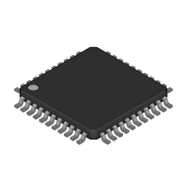
CY2V995AI Zero Delay Buffer, 200 MHz, 44-TQFP

MPNCY2V995AI
End of Life

Cypress CY2V995AI Zero Delay Buffer, PLL based clock driver, 200 MHz max, LVCMOS/LVTTL input, LVTTL output, 2:8 fanout, 44-TQFP, -40 to 85°C, dual supply 2.375V–2.625V / 2.97V–3.63V.

$4.38Ref. price · indicative, final on quote
Packaging44-TQFP
StockContact for availability
MOQ1 pcs
  • 100% new & originalTraceable channels only — no refurbs, no pulls, no remarked parts.
  • Date & lot codes on quoteStated per line before you commit; label photos on request.
  • MSL-compliant ESD packingMoisture-sealed bags with indicator cards; reels photo-verified.
  • PayPal buyer protectionPay by T/T, PayPal or Payoneer — card payments covered end to end.

Specifications

CY2V995AI Technical Specifications
ParameterValue
TypeZero Delay Buffer
Mounting typeSurface Mount
Voltage2.375V ~ 2.625V, 2.97V ~ 3.63V
Frequency200 MHz
Operating temperature-40°C ~ 85°C (TA)
InputLVCMOS, LVTTL
OutputLVTTL
PackageBulk
Case44-TQFP
Number of circuits1
Ratio - Input:Output2:8
Differential - Input:OutputNo/No

Product details

PLL-based zero delay buffer for clock distribution

The Cypress CY2V995AI is a PLL-based zero delay buffer designed to regenerate a clock signal with minimal phase shift between input and output. It accepts LVCMOS or LVTTL inputs and delivers LVTTL outputs across eight fanout paths from two input sources (2:8 ratio), making it a fit for distributing a clean, low-skew clock to multiple loads in a system. Rated for a maximum operating frequency of 200 MHz, this part suits clock trees in networking gear, base stations, test equipment, and industrial controllers where timing margin matters. The industrial temperature range of -40°C to 85°C covers outdoor telecom cabinets and factory-floor automation without requiring a commercial-grade workaround.

Supply voltage flexibility and package

The CY2V995AI operates from two distinct supply ranges: 2.375V to 2.625V and 2.97V to 3.63V. This dual-range support lets the same part work in a 2.5V or 3.3V logic environment without a separate voltage translator on the clock line — a BOM simplification when mixing FPGA banks and ASIC I/O. Housed in a 44-TQFP (10x10 mm) surface-mount package.

Lifecycle and sourcing posture

For a BOM line that needs a zero delay buffer, this part carries no near-term obsolescence risk. Note that the RoHS compliance status is marked non-compliant, so verify your assembly's exemption or waiver requirements for a lead-free reflow process.

Frequently asked questions

Is CY2V995AI a zero delay buffer?

Yes, the CY2V995AI is a PLL-based zero delay buffer. It regenerates the input clock with minimal phase offset, which is the defining function of this device class.

Does CY2V995AI support LVCMOS input?

Yes, the CY2V995AI accepts both LVCMOS and LVTTL input signals. Outputs are LVTTL.