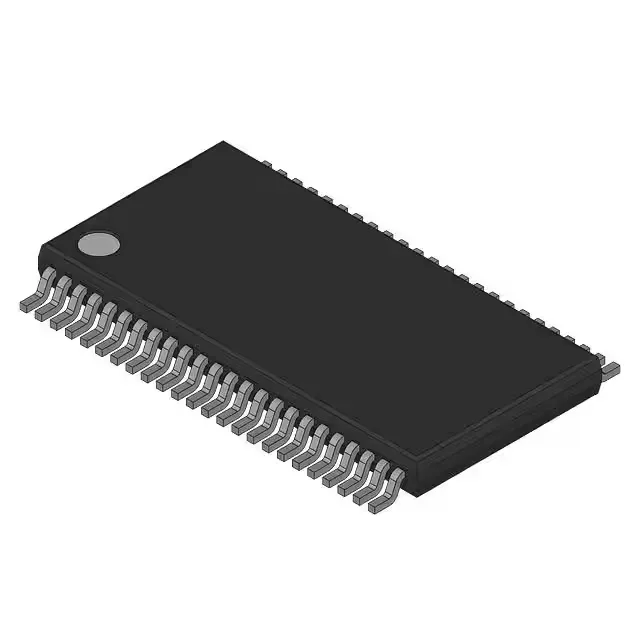
The 230 MHz maximum frequency is the clock rate the PLL can lock to and distribute with acceptable jitter. The 2:10 input-to-output ratio means one differential clock pair drives ten differential output pairs.
Differential I/O and PLL bypass — signal integrity options
Both the input and the outputs are differential (LVDS or similar levels), which gives common-mode noise rejection on the clock lines — important when routing near switching regulators or data buses on a multi-layer PCB. The PLL has a bypass mode, letting you feed the input clock straight through to the outputs if you need zero added latency or want to use an external clean clock source. That bypass feature is useful during board bring-up: you can isolate whether jitter comes from the PLL or from upstream clock generation.
Active lifecycle, but RoHS non-compliant — sourcing reality
However, it is marked RoHS non-compliant, meaning the device uses lead (Pb) in the solder finish or internal construction. This restricts its use in products destined for EU RoHS-regulated markets unless a specific exemption applies. For legacy designs that already have a leaded reflow profile, this is not an issue. For new designs targeting RoHS compliance, you will need a Pb-free alternate or a waiver.